SBOS935B April 2020 – July 2020 TLV197-Q1 , TLV2197-Q1 , TLV4197-Q1
PRODUCTION DATA.
- 1 Features
- 2 Applications
- 3 Description
- 4 Revision History
- 5 Pin Configuration and Functions
-
6 Specifications
- 6.1 Absolute Maximum Ratings
- 6.2 ESD Ratings
- 6.3 Recommended Operating Conditions
- 6.4 Thermal Information: TLV197-Q1
- 6.5 Thermal Information: TLV2197-Q1
- 6.6 Thermal Information: TLV4197-Q1
- 6.7 Electrical Characteristics: VS = ±4 V to ±18 V (VS = 8 V to 36 V)
- 6.8 Electrical Characteristics: VS = ±2.25 V to ±4 V (VS = 4.5 V to 8 V)
- 6.9 Typical Characteristics
- 7 Detailed Description
- 8 Application and Implementation
- 9 Power Supply Recommendations
- 10Layout
- 11Device and Documentation Support
- 12Mechanical, Packaging, and Orderable Information
7.3.7 Electrical Overstress
Designers often ask questions about the capability of an operational amplifier to withstand electrical overstress (EOS). These questions tend to focus on the device inputs, but may involve the supply voltage pins or even the output pin. Each of these different pin functions have electrical stress limits determined by the voltage breakdown characteristics of the particular semiconductor fabrication process and specific circuits connected to the pin. Additionally, internal electrostatic discharge (ESD) protection is built into these circuits to protect them from accidental ESD events both before and during product assembly.
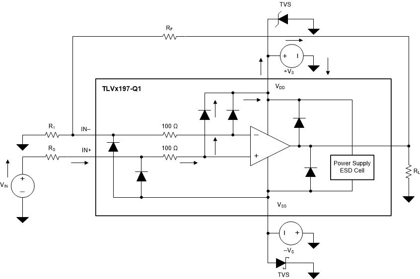
Having a good understanding of this basic ESD circuitry and its relevance to an electrical overstress event is helpful. Figure 40 shows an illustration of the ESD circuits contained in the TLVx197-Q1 (indicated by the dashed line area). The ESD protection circuitry involves several current-steering diodes connected from the input and output pins and routed back to the internal power-supply lines, where the diodes meet at an absorption device or the power-supply ESD cell, internal to the operational amplifier. This protection circuitry is intended to remain inactive during normal circuit operation.
 Figure 40. Equivalent Internal ESD Circuitry Relative to a Typical Circuit Application
 An ESD event is very short in duration and very high voltage (for example, 1 kV, 100 ns); whereas, an EOS event is long duration and lower voltage (for example, 50 V, 100 ms). The ESD diodes are designed for out-of-circuit ESD protection (that is, during assembly, test, and storage of the device before being soldered to the PCB). During an ESD event, the ESD signal is passed through the ESD steering diodes to an absorption circuit (labeled ESD power-supply circuit). The ESD absorption circuit clamps the supplies to a safe level.
Although this behavior is necessary for out-of-circuit protection, excessive current and damage is caused if activated in-circuit. A transient voltage suppressors (TVS) can be used to prevent against damage caused by turning on the ESD absorption circuit during an in-circuit ESD event. Using the appropriate current limiting resistors and TVS diodes allows for the use of device ESD diodes to protect against EOS events.