JAJSEM1F March 2001 – August 2016 TLV2370 , TLV2371 , TLV2372 , TLV2373 , TLV2374 , TLV2375
PRODUCTION DATA.
- 1 特長
- 2 アプリケーション
- 3 概要
- 4 改訂履歴
- 5 Device Comparison Tables
- 6 Pin Configuration and Functions
- 7 Specifications
- 8 Typical Characteristics
- 9 Detailed Description
- 10Application and Implementation
- 11Power Supply Recommendations
- 12Layout
- 13デバイスおよびドキュメントのサポート
- 14メカニカル、パッケージ、および注文情報
パッケージ・オプション
メカニカル・データ(パッケージ|ピン)
サーマルパッド・メカニカル・データ
発注情報
8 Typical Characteristics
Table 3. Table of Graphs
| FIGURE | |||
|---|---|---|---|
| VIO | Input offset voltage | vs Common-mode input voltage | Figure 1, Figure 2, Figure 3 |
| CMRR | Common-mode rejection ratio | vs Frequency | Figure 4 |
| Input bias and offset current | vs Free-air temperature | Figure 5 | |
| VOL | Low-level output voltage | vs Low-level output current | Figure 6, Figure 8, Figure 10 |
| VOH | High-level output voltage | vs High-level output current | Figure 7, Figure 9, Figure 11 |
| VO(PP) | Peak-to-peak output voltage | vs Frequency | Figure 12 |
| IDD | Supply current | vs Supply voltage | Figure 13 |
| PSRR | Power supply rejection ratio | vs Frequency | Figure 14 |
| AVD | Differential voltage gain and phase | vs Frequency | Figure 15 |
| Gain-bandwidth product | vs Free-air temperature | Figure 16 | |
| SR | Slew rate | vs Supply voltage | Figure 17 |
| vs Free-air temperature | Figure 18 | ||
| φm | Phase margin | vs Capacitive load | Figure 19 |
| Vn | Equivalent input noise voltage | vs Frequency | Figure 20 |
| Voltage-follower large-signal pulse response | Figure 21, Figure 22 | ||
| Voltage-follower small-signal pulse response | Figure 23 | ||
| Inverting large-signal response | Figure 24, Figure 25 | ||
| Inverting small-signal response | Figure 26 | ||
| Crosstalk | vs Frequency | Figure 27 | |
| Shutdown forward & reverse isolation | vs Frequency | Figure 28 | |
| IDD(SHDN) | Shutdown supply current | vs Supply voltage | Figure 29 |
| IDD(SHDN) | Shutdown pin leakage current | vs Shutdown pin voltage | Figure 30 |
| IDD(SHDN) | Shutdown supply current, output voltage | vs Time | Figure 31, Figure 32 |
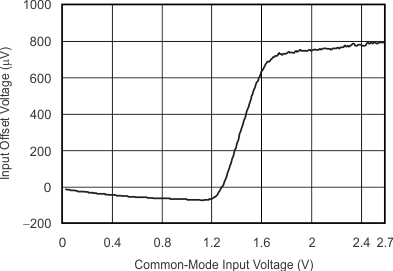 Figure 1. Input Offset Voltage vs Common-Mode Input Voltage
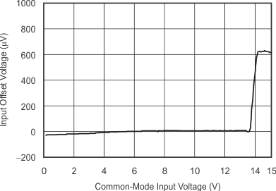 Figure 3. Input Offset Voltage vs Common-Mode Input Voltage
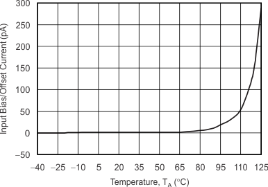 Figure 5. Input Bias or Offset Current vs Free-Air Temperature
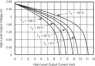 Figure 7. High-Level Output Voltage vs High-Level Output Current
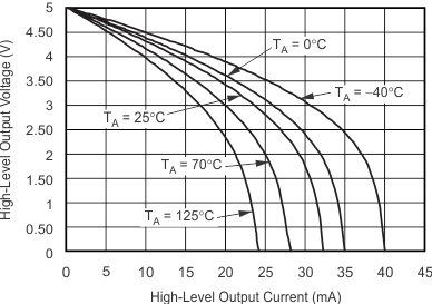 Figure 9. High-Level Output Voltage vs High-Level Output Current
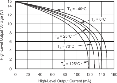 Figure 11. High-Level Output Voltage vs High-Level Output Current
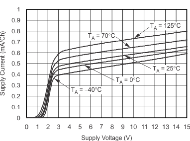 Figure 13. Supply Current vs Supply Voltage
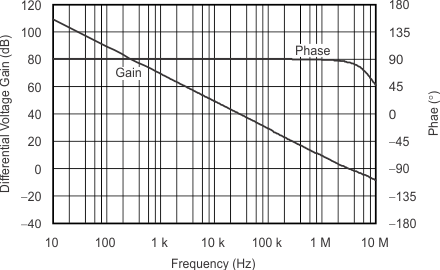 Figure 15. Differential Voltage Gain and Phase vs Frequency
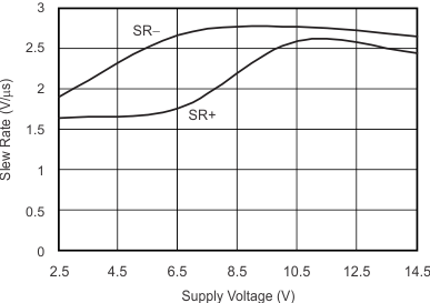 Figure 17. Slew Rate vs Supply Voltage
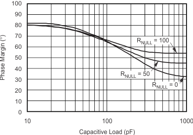 Figure 19. Phase Margin vs Capacitive Load
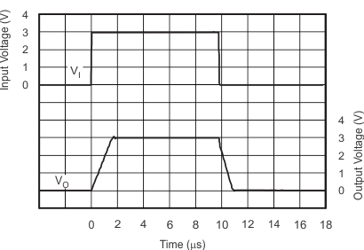 Figure 21. Voltage-Follower Large-Signal Pulse Response
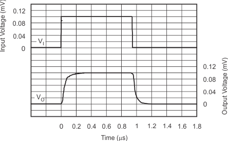 Figure 23. Voltage-Follower Small-Signal Pulse Response
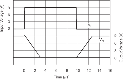 Figure 25. Inverting Large-Signal Response
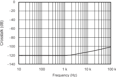 Figure 27. Crosstalk vs Frequency
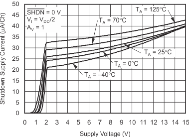 Figure 29. Shutdown Supply Current vs Supply Voltage
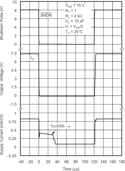 Figure 31. Shutdown Supply Current and Output Voltage vs Time
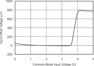 Figure 2. Input Offset Voltage vs Common-Mode Input Voltage
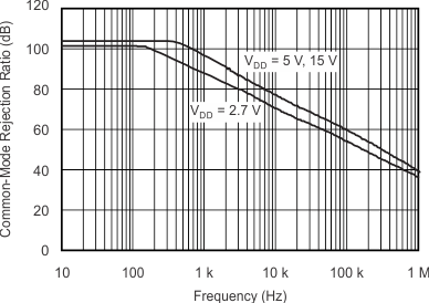 Figure 4. Common-Mode Rejection Ratio vs Frequency
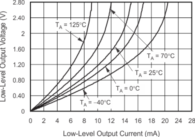 Figure 6. Low-Level Output Voltage vs Low-Level Output Current
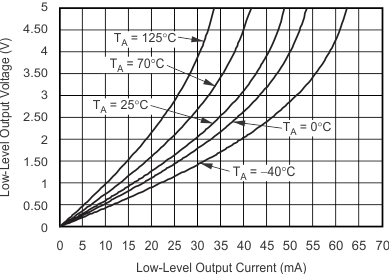 Figure 8. Low-Level Output Voltage vs Low-Level Output Current
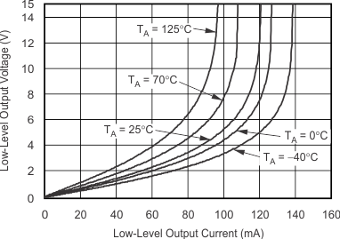 Figure 10. Low-Level Output Voltage vs Low-Level Output Current
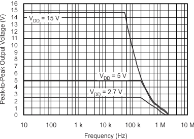 Figure 12. Peak-to-Peak Output Voltage vs Frequency
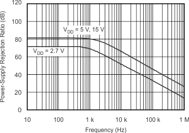 Figure 14. Power Supply Rejection Ratio vs Frequency
 Figure 16. Gain Bandwidth Product vs Free-Air Temperature
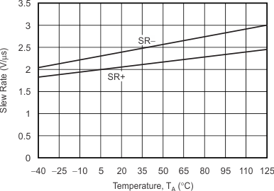 Figure 18. Slew Rate vs Free-Air Temperature
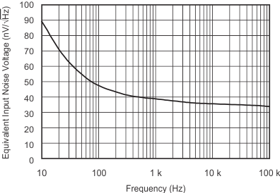 Figure 20. Equivalent Input Noise Voltage vs Frequency
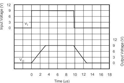 Figure 22. Voltage-Follower Large-Signal Pulse Response
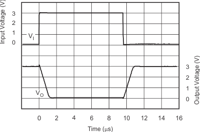 Figure 24. Inverting Large-Signal Response
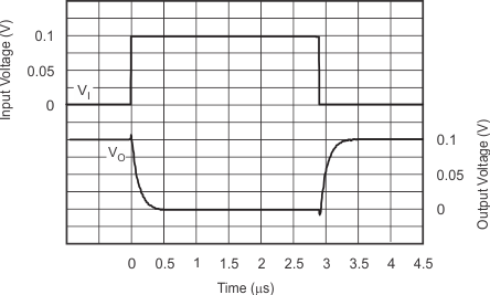 Figure 26. Inverting Small-Signal Response
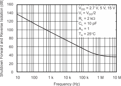 Figure 28. Shutdown Forward and Reverse Isolation vs Frequency
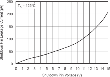 Figure 30. Shutdown Pin Leakage Current vs Shutdown Pin Voltage
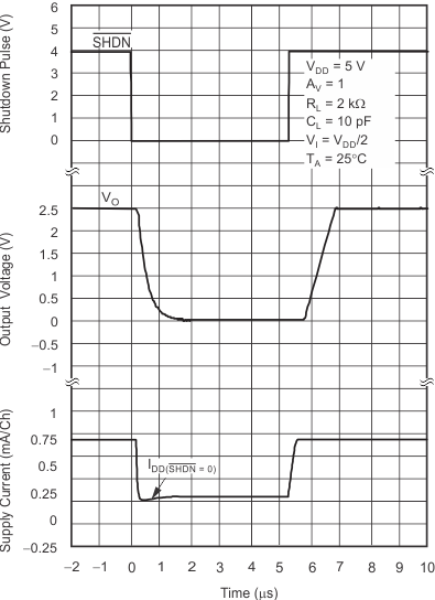 Figure 32. Shutdown Supply Current/output Voltage vs Time