-
TLV2553 12-Bit, 200-KSPS, 11-Channel, Low-Power, Serial ADC
- 1 Features
- 2 Applications
- 3 Description
- 4 Revision History
- 5 Pin Configuration and Functions
-
6 Specifications
- 6.1 Absolute Maximum Ratings
- 6.2 ESD Ratings
- 6.3 Recommended Operating Conditions
- 6.4 Thermal Information
- 6.5 Electrical Characteristics
- 6.6 External Reference Specifications
- 6.7 Operating Characteristics
- 6.8 Timing Requirements: VREF+ = 5 V
- 6.9 Timing Requirements: VREF+ = 2.5 V
- 6.10 Typical Characteristics
- 7 Parameter Measurement Information
-
8 Detailed Description
- 8.1 Overview
- 8.2 Functional Block Diagram
- 8.3 Feature Description
- 8.4
Device Functional Modes
- 8.4.1 Converter Operation
- 8.4.2 Data I/O Cycle
- 8.4.3 Sampling Cycle
- 8.4.4 Conversion Cycle
- 8.4.5 Power Up and Initialization
- 8.4.6 Data Input
- 8.4.7 Data Input—Address/Command Bits
- 8.4.8 Data Output Length
- 8.4.9 LSB Out First
- 8.4.10 Bipolar Output Format
- 8.4.11 EOC Output
- 8.4.12 Chip-Select Input (CS)
- 8.4.13 Power-Down Features
- 9 Application and Implementation
- 10Power Supply Recommendations
- 11Layout
- 12Device and Documentation Support
- 13Mechanical, Packaging, and Orderable Information
- IMPORTANT NOTICE
パッケージ・オプション
メカニカル・データ(パッケージ|ピン)
サーマルパッド・メカニカル・データ
発注情報
TLV2553 12-Bit, 200-KSPS, 11-Channel, Low-Power, Serial ADC
1 Features
- 12-Bit-Resolution A/D Converter
- Up to 200 KSPS (150 KSPS for 3 V) Throughput Over Operating Temperature Range With 12-Bit Output Mode
- 11 Analog Input Channels
- 3 Built-In Self-Test Modes
- Inherent Sample and Hold Function
- Linearity Error, ±1 LSB Maximum
- On-Chip Conversion Clock
- Unipolar or Bipolar Output Operation
- Programmable MSB or LSB First
- Programmable Power Down
- Programmable Output Data Length
- SPI Compatible Serial Interface With I/O Clock Frequencies up to 15 MHz (CPOL=0, CPHA=0)
2 Applications
- Process Control
- Portable Data Logging
- Battery-Powered Instruments
3 Description
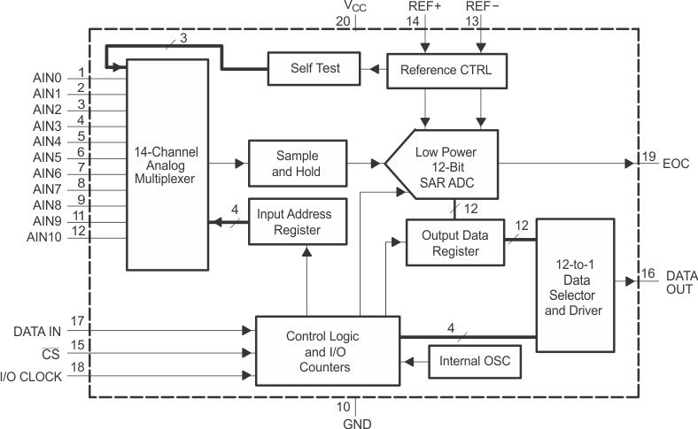
The TLV2553 is a 12-bit, switched-capacitor, successive-approximation, analog-to-digital converter. The ADC has three control inputs [chip select (CS), the input-output clock, and the address/control input (DATAIN)], designed for communication with the serial port of a host processor or peripheral through a serial 3-state output.
In addition to the high-speed converter and versatile control capability, the device has an on-chip 14-channel multiplexer that can select any one of 11 inputs or any one of three internal self-test voltages using configuration register 1. The sample-and-hold function is automatic. At the end of conversion, when programmed as EOC, the pin 19 output goes high to indicate that conversion is complete. The converter incorporated in the device features differential, high- impedance reference inputs that facilitate ratiometric conversion, scaling, and isolation of analog circuitry from logic and supply noise. A switched-capacitor design allows low-error conversion over the full operating temperature range.
The TLV2553I is characterized for operation from
TA = –40°C to 85°C.
Device Information(1)
| PART NUMBER | PACKAGE | BODY SIZE (NOM) |
|---|---|---|
| TLV2553IPW | TSSOP (20) | 6.50 mm × 4.40 mm |
| TLV2553IDW | SOIC (20) | 12.80 mm × 7.50 mm |
- For all available packages, see the orderable addendum at the end of the data sheet.
Block Diagram
4 Revision History
Changes from B Revision (September 2002) to C Revision
- ESD Ratings table, Feature Description section, Device Functional Modes, Application and Implementation section, Power Supply Recommendations section, Layout section, Device and Documentation Support section, and Mechanical, Packaging, and Orderable Information sectionGo
- Deleted Available Options tableGo
- Deleted Lead temperature row from Absolute Maximum Ratings Go
5 Pin Configuration and Functions
Pin Functions
| PIN | I/O | DESCRIPTION | |
|---|---|---|---|
| NAME | NO. | ||
| AIN0 to AIN10 | 1 to 9, 11, 12 | I | Analog input. These 11 analog-signal inputs are internally multiplexed. |
| CS | 15 | I | Chip select. A high-to-low transition on CS resets the internal counters and controls and enables DATA OUT, DATA IN, and I/O CLOCK. A low-to-high transition disables DATA IN and I/O CLOCK within a setup time. |
| DATA IN | 17 | I | Serial data input. The 4-bit serial data can be used as address selects the desired analog input channel or test voltage to be converted next, or a command to activate other features. The input data is presented with the MSB (D7) first and is shifted in on the first four rising edges of the I/O CLOCK. After the four address/command bits are read into the command register CMR, I/O CLOCK clocks the remaining four bits of configuration in. |
| DATA OUT | 16 | O | 3-state serial output for the A/D conversion result. DATA OUT is in the high-impedance state when CS is high and active when CS is low. With a valid CS, DATA OUT is removed from the high-impedance state and is driven to the logic level corresponding to the MSB/LSB value of the previous conversion result. The next falling edge of I/O CLOCK drives DATA OUT to the logic level corresponding to the next MSB/LSB, and the remaining bits are shifted out in order. |
| EOC | 19 | O | End-of-convertions status. Used to indicate the end of conversion (EOC) to the host processor. EOC goes from a high to a low logic level after the falling edge of the last I/O CLOCK and remains low until the conversion is complete and the data is ready for transfer. |
| GND | 10 | — | Ground. GND is the ground return terminal for the internal circuitry. Unless otherwise noted, all voltage measurements are with respect to GND. |
| I/O CLOCK | 18 | I |
Input /output clock. I/O CLOCK receives the serial input and performs the following four functions:
|
| REF+ | 14 | I/O | Positive reference voltage The upper reference voltage value (nominally VCC) is applied to REF+. The maximum analog input voltage range is determined by the difference between the voltage applied to terminals REF+ and REF–. |
| REF– | 13 | I/O | Negative reference voltage. The lower reference voltage value (nominally ground) is applied to REF–. This pin is connected to analog ground (GND of the ADC) when internal reference is used. |
| VCC | 20 | — | Positive supply voltage |
6 Specifications
6.1 Absolute Maximum Ratings
over operating free-air temperature range (unless otherwise noted)(1)| MIN | MAX | UNIT | ||
|---|---|---|---|---|
| VCC | Supply voltage(2) | –0.5 | 6.5 | V |
| VI | Input voltage (any input) | –0.3 | VCC + 0.3 | |
| VO | Output voltage | –0.3 | VCC + 0.3 | |
| Vref+ | Positive reference voltage | –0.3 | VCC + 0.3 | |
| Vref– | Negative reference voltage | –0.3 | VCC + 0.3 | |
| II | Peak input current (any input) | –20 | 20 | mA |
| Peak total input current (all inputs) | –30 | 30 | ||
| TJ | Operating virtual junction temperature | –40 | 150 | °C |
| TA | Operating free-air temperature | –40 | 85 | |
| Tstg | Storage temperature | –65 | 150 | |
6.2 ESD Ratings
| VALUE | UNIT | |||
|---|---|---|---|---|
| V(ESD) | Electrostatic discharge | Human-body model (HBM), per ANSI/ESDA/JEDEC JS-001(1) | ±2000 | V |
| Charged-device model (CDM), per JEDEC specification JESD22-C101(2) | ±500 | |||
6.3 Recommended Operating Conditions
over operating free-air temperature range (unless otherwise noted)| MIN | NOM | MAX | UNIT | ||||
|---|---|---|---|---|---|---|---|
| VCC | Supply voltage | 2.7 | 5.5 | V | |||
| I/O CLOCK frequency | VCC = 4.5 V to 5.5 V | 16-bit I/O | 0.01 | 15 | MHz | ||
| 12-bit I/O | 0.01 | 15 | |||||
| 8-bit I/O | 0.01 | 15 | |||||
| VCC = 2.7 V to 3.6 V | 0.01 | 10 | |||||
| I/O CLOCK | Tolerable clock jitter | VCC = 4.5 V to 5.5 V | 0.38 | ns | |||
| Aperature jitter | VCC = 4.5 V to 5.5 V | 100 | ps | ||||
| Analog input voltage(1) | VCC = 4.5 V to 5.5 V | 0 | (REF+ ) – (REF– ) | V | |||
| VCC = 3 V to 3.6 V | 0 | (REF+ ) – (REF– ) | |||||
| VCC = 2.7 V to 3 V | 0 | (REF+ ) – (REF– ) | |||||
| VIH | High-level control input voltage | VCC = 4.5 V to 5.5 V | 2 | V | |||
| VCC = 2.7 V to 3.6 V | 2.1 | ||||||
| VIL | Low-level control input voltage | VCC = 4.5 V to 5.5 V | 0.8 | V | |||
| VCC = 2.7 V to 3.6 V | 0.6 | ||||||
| TA | Operating free-air temperature | TLV2553I | –40 | 85 | °C | ||
6.4 Thermal Information
| THERMAL METRIC(1) | TLV2553 | UNIT | ||
|---|---|---|---|---|
| DW (SOIC) | PW (TSSOP) | |||
| 20 PINS | 20 PINS | |||
| RθJA | Junction-to-ambient thermal resistance | 66 | 88.1 | °C/W |
| RθJC(top) | Junction-to-case (top) thermal resistance | 31.4 | 21.6 | °C/W |
| RθJB | Junction-to-board thermal resistance | 33.7 | 40.4 | °C/W |
| ψJT | Junction-to-top characterization parameter | 7.4 | 0.8 | °C/W |
| ψJB | Junction-to-board characterization parameter | 33.3 | 39.7 | °C/W |
6.5 Electrical Characteristics
over recommended operating free-air temperature range, when VCC = 5 V: VREF+ = 5 V, I/O CLOCK frequency = 15 MHz, when VCC = 2.7 V: VREF+ = 2.5 V, I/O CLOCK frequency = 10 MHz (unless otherwise noted)| PARAMETER | TEST CONDITIONS | MIN | TYP(1) | MAX | UNIT | ||||
|---|---|---|---|---|---|---|---|---|---|
| VOH | High-level output voltage | VCC = 4.5 V, IOH = –1.6 mA VCC = 2.7 V, IOH = –0.2 mA |
30 pF | 2.4 | V | ||||
| VCC = 4.5 V, IOH = –20 μA VCC = 2.7 V, IOH = –20 μA |
VCC – 0.1 | ||||||||
| VOL | Low-level output voltage | VCC = 4.5 V, IOL = –1.6 mA VCC = 2.7 V, IOL = –0.8 mA |
30 pF | 0.4 | V | ||||
| VCC = 4.5 V, IOL = –20 μA VCC = 2.7 V, IOL = –20 μA |
0.1 | ||||||||
| IOZ | High-impedance off-state output current | VO = VCC, CS = VCC | 1 | 2.5 | μA | ||||
| VO = 0 V, CS = VCC | –1 | –2.5 | |||||||
| ICC | Operating supply current | CS = 0 V, External reference | VCC = 5 V | 1.2 | mA | ||||
| VCC = 2.7 V | 0.9 | ||||||||
| ICC(PD) | Power-down current | For all digital inputs, 0 ≤ VI ≤ 0.5 V or VI ≥ VCC – 0.5 V, I/O CLOCK = 0 V | Software power down | 0.1 | 1 | μA | |||
| Auto power down | 0.1 | 10 | |||||||
| IIH | High-level input current | VI = VCC | 0.005 | 2.5 | μA | ||||
| IIL | Low-level input current | VI = 0 V | –0.005 | –2.5 | μA | ||||
| Ilkg | Selected channel leakage current | Selected channel at VCC , Unselected channel at 0 V |
1 | μA | |||||
| Selected channel at 0 V, Unselected channel at VCC |
–1 | ||||||||
| fOSC | Internal oscillator frequency | VCC = 4.5 V to 5.5 V | 3.27 | MHz | |||||
| VCC = 2.7 V to 3.6 V | 2.56 | ||||||||
| tconvert | Conversion time (13.5 × (1/fOSC) + 25 ns) |
VCC = 4.5 V to 5.5 V | 4.15 | μs | |||||
| VCC = 2.7 V to 3.6 V | 5.54 | ||||||||
| Internal oscillator frequency voltage | 3.6 | 4.1 | V | ||||||
| Zi | Input impedance(2) | Analog inputs | VCC = 4.5 V | 500 | Ω | ||||
| VCC = 2.7 V | 600 | ||||||||
| Ci | Input capacitance | Analog inputs | 45 | 55 | pF | ||||
| Control inputs | 5 | 15 | |||||||
6.6 External Reference Specifications
| PARAMETER | TEST CONDITIONS | MIN | TYP(1) | MAX | UNIT | ||
|---|---|---|---|---|---|---|---|
| REF– | Reference input voltage | VCC = 4.5 V to 5.5 V | –0.1 | 0 | 0.1 | V | |
| VCC = 2.7 V to 3.6 V | –0.1 | 0 | 0.1 | ||||
| REF+ | Reference input voltage | VCC = 4.5 V to 5.5 V | 2 | VCC | V | ||
| VCC = 2.7 V to 3.6 V | 2 | VCC | |||||
| External reference input voltage difference, (REF+) – (REF–)(2) | VCC = 4.5 V to 5.5 V | 1.9 | VCC | V | |||
| VCC = 2.7 V to 3.6 V | 1.9 | VCC | |||||
| External reference supply current | CS at 0 V | VCC = 4.5 V to 5.5 V | 0.94 | mA | |||
| VCC = 2.7 V to 3.6 V | 0.62 | ||||||
| Reference input impedance | VCC = 5 V | Static | 1 | MΩ | |||
| During sampling/conversion | 6 | 9 | kΩ | ||||
| VCC = 2.7 V | Static | 1 | MΩ | ||||
| During sampling/conversion | 6 | 9 | kΩ | ||||
6.7 Operating Characteristics
over recommended operating free-air temperature range, VREF+ = 5 V, I/O CLOCK frequency = 15 MHz when VCC = 5 V, VREF+ = 2.5 V, I/O CLOCK frequency = 10 MHz when VCC = 2.7 V (unless otherwise noted)| PARAMETER | TEST CONDITIONS | MIN | TYP(1) | MAX | UNIT | |
|---|---|---|---|---|---|---|
| INL | Integral linearity error(3) | –1 | 1 | LSB | ||
| DNL | Differential linearity error | –1 | 1 | LSB | ||
| EO | Offset error(4) | See (2) | –2 | 2 | mV | |
| EQ | Gain error(4) | See(2) | –3 | 3 | mV | |
| ET | Total unadjusted error(5) | ±15 | LSB | |||
| Self-test output code Table 2, (6) | Address data input = 1011 | 2048 | ||||
| Address data input = 1100 | 0 | |||||
| Address data input = 1101 | 4095 | |||||
6.8 Timing Requirements: VREF+ = 5 V
over recommended operating free-air temperature range, I/O CLOCK frequency = 15 MHz, VCC = 5 V, load = 25 pF (unless otherwise noted)| MIN | TYP | MAX | UNIT | |||
|---|---|---|---|---|---|---|
| tw1 | Pulse duration I/O CLOCK high or low | 26.7 | 100000 | ns | ||
| tsu1 | Setup time DATA IN valid before I/O CLOCK rising edge (see Figure 32) | 12 | ns | |||
| th1 | Hold time DATA IN valid after I/O CLOCK rising edge (see Figure 32) | 0 | ns | |||
| tsu2 | Setup time CS low before first rising I/O CLOCK edge(1) (see Figure 33) | 25 | ns | |||
| th2 | Hold time CS pulse duration high time (see Figure 33) | 100 | ns | |||
| th3 | Hold time CS low after last I/O CLOCK falling edge (see Figure 33) | 0 | ns | |||
| th4 | Hold time DATA OUT valid after I/O CLOCK falling edge (see Figure 34) | 2 | ns | |||
| th5 | Hold time CS high after EOC rising edge when CS is toggled (see Figure 37) | 0 | ns | |||
| td1 | Delay time CS falling edge to DATA OUT valid (MSB or LSB) (see Figure 31) | Load = 25 pF | 28 | ns | ||
| Load = 10 pF | 20 | ns | ||||
| td2 | Delay time CS rising edge to DATA OUT high impedance (see Figure 31) | 10 | ns | |||
| td3 | Delay time I/O CLOCK falling edge to next DATA OUT bit valid (see Figure 34) | 2 | 20 | ns | ||
| td4 | Delay time Last I/O CLOCK falling edge to EOC falling edge | 55 | ns | |||
| td5 | Delay time last I/O CLOCK falling edge to CS falling edge to abort conversion | 1.5 | µs | |||
| tt1 | Transition time I/O CLOCK (1)(see Figure 34) | 1 | µs | |||
| tt2 | Transition time DATA OUT (see Figure 34) | 5 | ns | |||
| tt3 | Transition time INT/EOC, CL at 7 pF (see Figure 36) | 2.4 | ns | |||
| tt4 | Transition time DATA IN, CS | 10 | µs | |||
| tcycle | Total cycle time (sample, conversion and delays)(1) | MAX(tconvert) + I/O period (8/12/16 CLKs) | µs | |||
| tsample | Channel acquisition time (sample), at 1 kΩ,(1) (See Figure 1 through Figure 6) | Source impedance = 25 Ω | 600 | ns | ||
| Source impedance = 100 Ω | 650 | |||||
| Source impedance = 500 Ω | 700 | |||||
| Source impedance = 1 kΩ | 1000 | |||||
6.9 Timing Requirements: VREF+ = 2.5 V
over recommended operating free-air temperature range, I/O CLOCK frequency = 10 MHz, VCC = 2.7 V, load = 25 pF (unless otherwise noted)| MIN | TYP | MAX | UNIT | |||
|---|---|---|---|---|---|---|
| tw1 | Pulse duration I/O CLOCK high or low | 40 | 100000 | ns | ||
| tsu1 | Setup time DATA IN valid before I/O CLOCK rising edge (see Figure 32) | 22 | ns | |||
| th1 | Hold time DATA IN valid after I/O CLOCK rising edge (see Figure 32) | 0 | ns | |||
| tsu2 | Setup time CS low before first rising I/O CLOCK edge(1) (see Figure 33) | 33 | ns | |||
| th2 | Hold time CS pulse duration high time (see Figure 33) | 100 | ns | |||
| th3 | Hold time CS low after last I/O CLOCK falling edge (see Figure 33) | 0 | ns | |||
| th4 | Hold time DATA OUT valid after I/O CLOCK falling edge (see Figure 33) | 2 | ns | |||
| th5 | Hold time CS high after EOC rising edge when CS is toggled (see Figure 37) | 0 | ns | |||
| td1 | Delay time CS falling edge to DATA OUT valid (MSB or LSB) (see Figure 31) | Load = 25 pF | 30 | ns | ||
| Load = 10 pF | 22 | ns | ||||
| td2 | Delay time CS rising edge to DATA OUT high impedance (see Figure 31) | 10 | ns | |||
| td3 | Delay time I/O CLOCK falling edge to next DATA OUT bit valid (see Figure 34) | 2 | 33 | ns | ||
| td4 | Delay time Last I/O CLOCK falling edge to EOC falling edge | 75 | ns | |||
| td5 | Delay time last I/O CLOCK falling edge to CS falling edge to abort conversion | 1.5 | µs | |||
| tt1 | Transition time I/O CLOCK (1)(see Figure 34) | 1 | µs | |||
| tt2 | Transition time DATA OUT (see Figure 34) | 5 | ns | |||
| tt3 | Transition time INT/EOC, CL at 7 pF (see Figure 36) | 4 | ns | |||
| tt4 | Transition time DATA IN, CS | 10 | µs | |||
| tcycle | Total cycle time (sample, conversion and delays)(1) | MAX(tconvert) + I/O period (8/12/16 CLKs) | µs | |||
| tsample | Channel acquisition time (sample), at 1 kΩ,(1) (See Figure 1 through Figure 6) | Source impedance = 25 Ω | 800 | ns | ||
| Source impedance = 100 Ω | 850 | |||||
| Source impedance = 500 Ω | 1000 | |||||
| Source impedance = 1 kΩ | 1600 | |||||
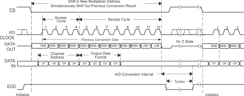 Figure 1. Timing for 12-Clock Transfer Using CS With DATA OUT Set for MSB First
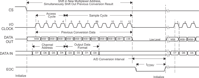
NOTE:
To minimize errors caused by noise at CS, the internal circuitry waits for a setup time after the CS falling edge before responding to control input signals. Therefore, no attempt should be made to clock in an address until the minimum CS setup time has elapsed.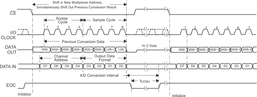 Figure 3. Timing for 8-Clock Transfer Using CS With DATA OUT Set for MSB First
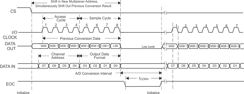
NOTE:
To minimize errors caused by noise at CS, the internal circuitry waits for a setup time after the CS falling edge before responding to control input signals. Therefore, no attempt should be made to clock in an address until the minimum CS setup time has elapsed.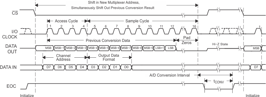 Figure 5. Timing for 16-Clock Transfer Using CS With DATA OUT Set for MSB First
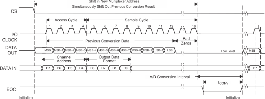
NOTE:
To minimize errors caused by noise at CS, the internal circuitry waits for a setup time after the CS falling edge before responding to control input signals. Therefore, no attempt should be made to clock in an address until the minimum CS setup time has elapsed.6.10 Typical Characteristics
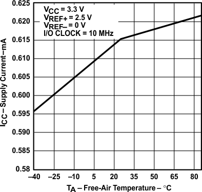
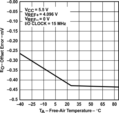
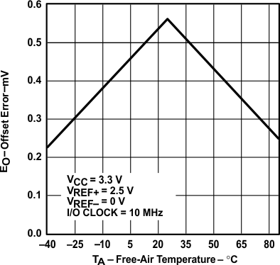
vs Free-Air Temperature
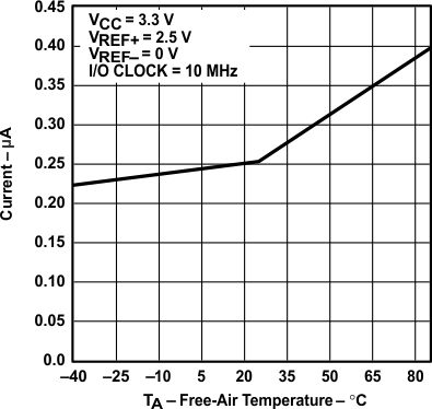
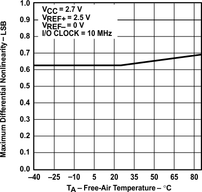
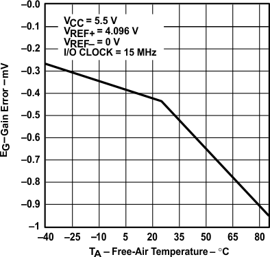
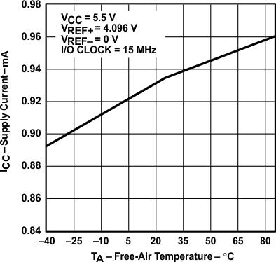
vs Free-air Temperature
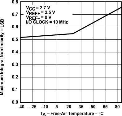
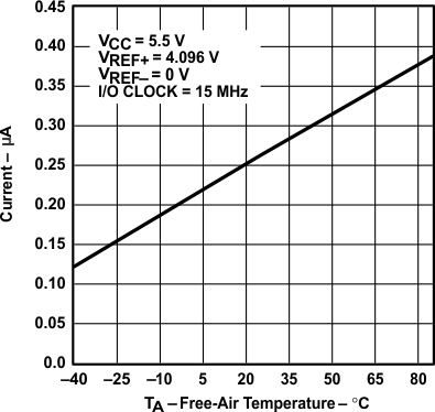
vs Free-air Temperature
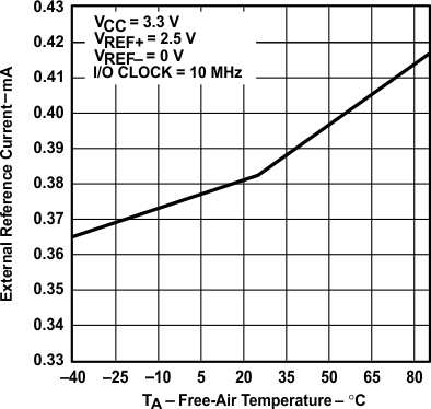
vs Free-air Temperature
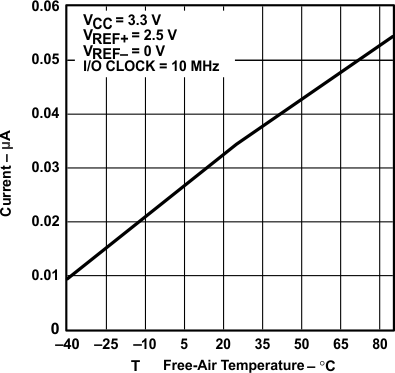
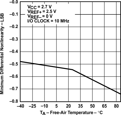
vs Free-air Temperature
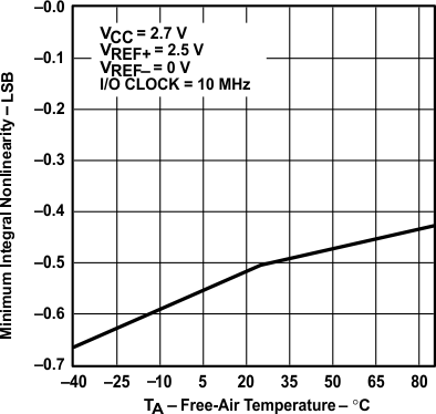
vs Free-air Temperature
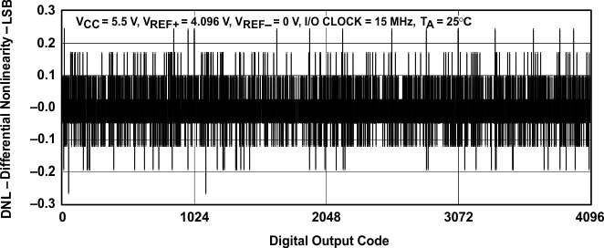
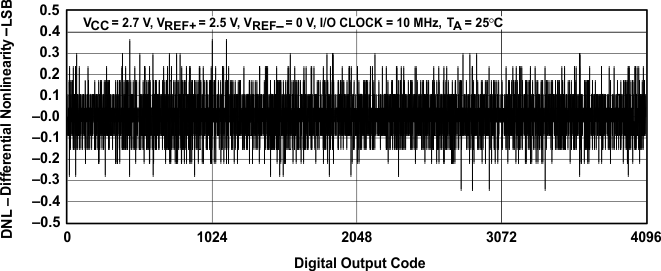 Figure 15. Differential Nonlinearity vs Digital Output Code
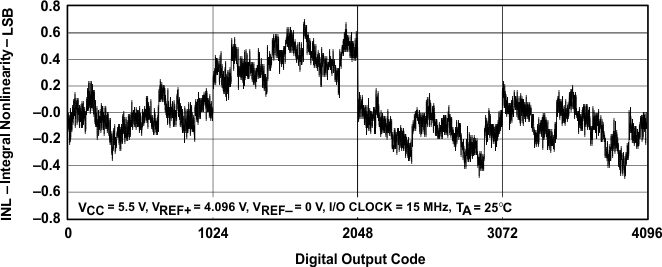
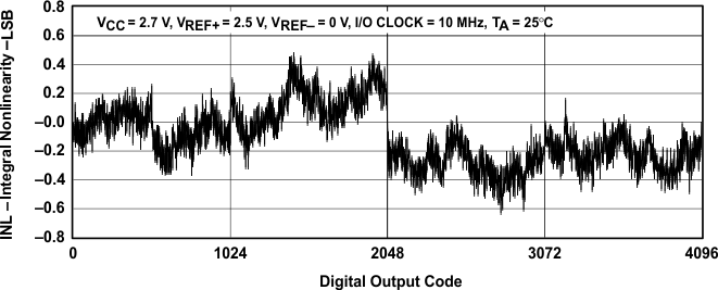 Figure 16. Integral Nonlinearity vs Digital Output Code
vs Free-air Temperature
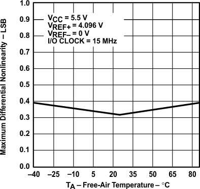
vs Free-air Temperature
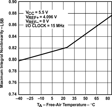
vs Free-air Temperature
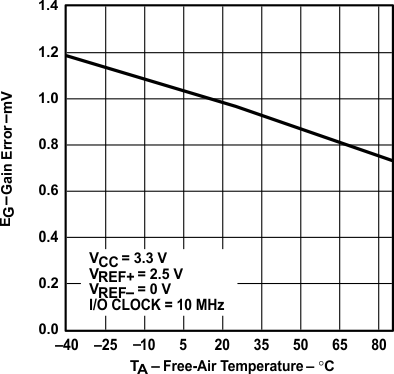
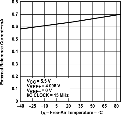
vs Free-air Temperature
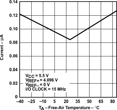
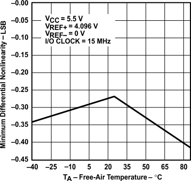
vs Free-air Temperature
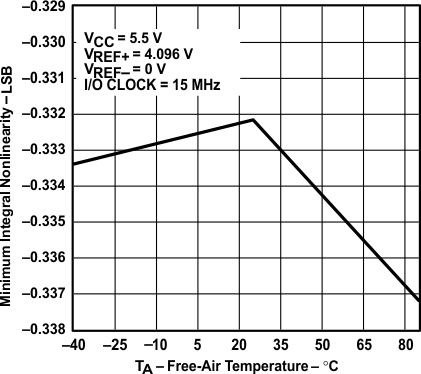
vs Free-air Temperature
