JAJSCS9B November 2016 – August 2017 TLV2316-Q1 , TLV316-Q1 , TLV4316-Q1
PRODUCTION DATA.
- 1 特長
- 2 アプリケーション
- 3 概要
- 4 改訂履歴
- 5 Device Comparison Table
- 6 Pin Configuration and Functions
- 7 Specifications
- 8 Detailed Description
- 9 Application and Implementation
- 10Power Supply Recommendations
- 11Layout
- 12デバイスおよびドキュメントのサポート
- 13メカニカル、パッケージ、および注文情報
9 Application and Implementation
NOTE
Information in the following applications sections is not part of the TI component specification, and TI does not warrant its accuracy or completeness. TI’s customers are responsible for determining suitability of components for their purposes. Customers should validate and test their design implementation to confirm system functionality.
9.1 Application Information
The TLV316-Q1, TLV2316-Q1, and TLV4316-Q1 devices are powered on when the supply is connected. The devices can operate as a single-supply operational amplifier or a dual-supply amplifier, depending on the application.
9.2 System Examples
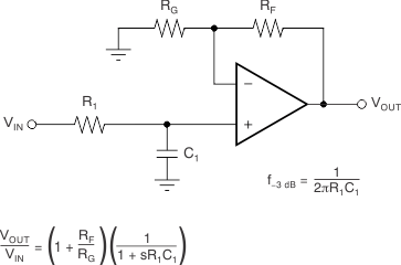
When receiving low-level signals, the device often requires limiting the bandwidth of the incoming signals into the system. The simplest way to establish this limited bandwidth is to place an RC filter at the noninverting pin of the amplifier, as shown in Figure 15.
 Figure 15. Single-Pole, Low-Pass Filter
If even more attenuation is needed, the device requires a multiple-pole filter. The Sallen-Key filter can be used for this task, as shown in Figure 16. For best results, the amplifier must have a bandwidth that is eight to ten times the filter frequency bandwidth. Failure to follow this guideline can result in a phase shift of the amplifier.
 Figure 16. Two-Pole, Low-Pass, Sallen-Key Filter