JAJSHP6A July 2019 – October 2019 TLV320ADC6140
PRODUCTION DATA.
- 1 特長
- 2 アプリケーション
- 3 概要
- 4 改訂履歴
- 5 概要(続き)
- 6 デバイス比較表
- 7 Pin Configuration and Functions
-
8 Specifications
- 8.1 Absolute Maximum Ratings
- 8.2 ESD Ratings
- 8.3 Recommended Operating Conditions
- 8.4 Thermal Information
- 8.5 Electrical Characteristics
- 8.6 Timing Requirements: I2C Interface
- 8.7 Switching Characteristics: I2C Interface
- 8.8 Timing Requirements: SPI Interface
- 8.9 Switching Characteristics: SPI Interface
- 8.10 Timing Requirements: TDM, I2S or LJ Interface
- 8.11 Switching Characteristics: TDM, I2S or LJ Interface
- 8.12 Timing Requirements: PDM Digital Microphone Interface
- 8.13 Switching Characteristics: PDM Digial Microphone Interface
- 8.14 Typical Characteristics
-
9 Detailed Description
- 9.1 Overview
- 9.2 Functional Block Diagram
- 9.3
Feature Description
- 9.3.1 Serial Interfaces
- 9.3.2 Phase-Locked Loop (PLL) and Clock Generation
- 9.3.3 Input Channel Configurations
- 9.3.4 Reference Voltage
- 9.3.5 Programmable Microphone Bias
- 9.3.6
Signal-Chain Processing
- 9.3.6.1 Programmable Channel Gain and Digital Volume Control
- 9.3.6.2 Programmable Channel Gain Calibration
- 9.3.6.3 Programmable Channel Phase Calibration
- 9.3.6.4 Programmable Digital High-Pass Filter
- 9.3.6.5 Programmable Digital Biquad Filters
- 9.3.6.6 Programmable Channel Summer and Digital Mixer
- 9.3.6.7
Configurable Digital Decimation Filters
- 9.3.6.7.1
Linear Phase Filters
- 9.3.6.7.1.1 Sampling Rate: 8 kHz or 7.35 kHz
- 9.3.6.7.1.2 Sampling Rate: 16 kHz or 14.7 kHz
- 9.3.6.7.1.3 Sampling Rate: 24 kHz or 22.05 kHz
- 9.3.6.7.1.4 Sampling Rate: 32 kHz or 29.4 kHz
- 9.3.6.7.1.5 Sampling Rate: 48 kHz or 44.1 kHz
- 9.3.6.7.1.6 Sampling Rate: 96 kHz or 88.2 kHz
- 9.3.6.7.1.7 Sampling Rate: 192 kHz or 176.4 kHz
- 9.3.6.7.1.8 Sampling Rate: 384 kHz or 352.8 kHz
- 9.3.6.7.1.9 Sampling Rate 768 kHz or 705.6 kHz
- 9.3.6.7.2 Low-Latency Filters
- 9.3.6.7.3
Ultra-Low-Latency Filters
- 9.3.6.7.3.1 Sampling Rate: 16 kHz or 14.7 kHz
- 9.3.6.7.3.2 Sampling Rate: 24 kHz or 22.05 kHz
- 9.3.6.7.3.3 Sampling Rate: 32 kHz or 29.4 kHz
- 9.3.6.7.3.4 Sampling Rate: 48 kHz or 44.1 kHz
- 9.3.6.7.3.5 Sampling Rate: 96 kHz or 88.2 kHz
- 9.3.6.7.3.6 Sampling Rate 192 kHz or 176.4 kHz
- 9.3.6.7.3.7 Sampling Rate 384 kHz or 352.8 kHz
- 9.3.6.7.1
Linear Phase Filters
- 9.3.7 Dynamic Range Enhancer (DRE)
- 9.3.8 Automatic Gain Controller (AGC)
- 9.3.9 Digital PDM Microphone Record Channel
- 9.3.10 Interrupts, Status, and Digital I/O Pin Multiplexing
- 9.4 Device Functional Modes
- 9.5 Programming
- 9.6
Register Maps
- 9.6.1
Device Configuration Registers
- 9.6.1.1
Register Descriptions
- 9.6.1.1.1 PAGE_CFG Register (page = 0x00, address = 0x00) [reset = 0h]
- 9.6.1.1.2 SW_RESET Register (page = 0x00, address = 0x01) [reset = 0h]
- 9.6.1.1.3 SLEEP_CFG Register (page = 0x00, address = 0x02) [reset = 0h]
- 9.6.1.1.4 SHDN_CFG Register (page = 0x00, address = 0x05) [reset = 5h]
- 9.6.1.1.5 ASI_CFG0 Register (page = 0x00, address = 0x07) [reset = 30h]
- 9.6.1.1.6 ASI_CFG1 Register (page = 0x00, address = 0x08) [reset = 0h]
- 9.6.1.1.7 ASI_CFG2 Register (page = 0x00, address = 0x09) [reset = 0h]
- 9.6.1.1.8 ASI_CH1 Register (page = 0x00, address = 0x0B) [reset = 0h]
- 9.6.1.1.9 ASI_CH2 Register (page = 0x00, address = 0x0C) [reset = 1h]
- 9.6.1.1.10 ASI_CH3 Register (page = 0x00, address = 0x0D) [reset = 2h]
- 9.6.1.1.11 ASI_CH4 Register (page = 0x00, address = 0x0E) [reset = 3h]
- 9.6.1.1.12 ASI_CH5 Register (page = 0x00, address = 0x0F) [reset = 4h]
- 9.6.1.1.13 ASI_CH6 Register (page = 0x00, address = 0x10) [reset = 5h]
- 9.6.1.1.14 ASI_CH7 Register (page = 0x00, address = 0x11) [reset = 6h]
- 9.6.1.1.15 ASI_CH8 Register (page = 0x00, address = 0x12) [reset = 7h]
- 9.6.1.1.16 MST_CFG0 Register (page = 0x00, address = 0x13) [reset = 2h]
- 9.6.1.1.17 MST_CFG1 Register (page = 0x00, address = 0x14) [reset = 48h]
- 9.6.1.1.18 ASI_STS Register (page = 0x00, address = 0x15) [reset = FFh]
- 9.6.1.1.19 CLK_SRC Register (page = 0x00, address = 0x16) [reset = 10h]
- 9.6.1.1.20 PDMCLK_CFG Register (page = 0x00, address = 0x1F) [reset = 40h]
- 9.6.1.1.21 PDMIN_CFG Register (page = 0x00, address = 0x20) [reset = 0h]
- 9.6.1.1.22 GPIO_CFG0 Register (page = 0x00, address = 0x21) [reset = 22h]
- 9.6.1.1.23 GPO_CFG0 Register (page = 0x00, address = 0x22) [reset = 0h]
- 9.6.1.1.24 GPO_CFG1 Register (page = 0x00, address = 0x23) [reset = 0h]
- 9.6.1.1.25 GPO_CFG2 Register (page = 0x00, address = 0x24) [reset = 0h]
- 9.6.1.1.26 GPO_CFG3 Register (page = 0x00, address = 0x25) [reset = 0h]
- 9.6.1.1.27 GPO_VAL Register (page = 0x00, address = 0x29) [reset = 0h]
- 9.6.1.1.28 GPIO_MON Register (page = 0x00, address = 0x2A) [reset = 0h]
- 9.6.1.1.29 GPI_CFG0 Register (page = 0x00, address = 0x2B) [reset = 0h]
- 9.6.1.1.30 GPI_CFG1 Register (page = 0x00, address = 0x2C) [reset = 0h]
- 9.6.1.1.31 GPI_MON Register (page = 0x00, address = 0x2F) [reset = 0h]
- 9.6.1.1.32 INT_CFG Register (page = 0x00, address = 0x32) [reset = 0h]
- 9.6.1.1.33 INT_MASK0 Register (page = 0x00, address = 0x33) [reset = FFh]
- 9.6.1.1.34 INT_LTCH0 Register (page = 0x00, address = 0x36) [reset = 0h]
- 9.6.1.1.35 BIAS_CFG Register (page = 0x00, address = 0x3B) [reset = 0h]
- 9.6.1.1.36 CH1_CFG0 Register (page = 0x00, address = 0x3C) [reset = 0h]
- 9.6.1.1.37 CH1_CFG1 Register (page = 0x00, address = 0x3D) [reset = 0h]
- 9.6.1.1.38 CH1_CFG2 Register (page = 0x00, address = 0x3E) [reset = C9h]
- 9.6.1.1.39 CH1_CFG3 Register (page = 0x00, address = 0x3F) [reset = 80h]
- 9.6.1.1.40 CH1_CFG4 Register (page = 0x00, address = 0x40) [reset = 0h]
- 9.6.1.1.41 CH2_CFG0 Register (page = 0x00, address = 0x41) [reset = 0h]
- 9.6.1.1.42 CH2_CFG1 Register (page = 0x00, address = 0x42) [reset = 0h]
- 9.6.1.1.43 CH2_CFG2 Register (page = 0x00, address = 0x43) [reset = C9h]
- 9.6.1.1.44 CH2_CFG3 Register (page = 0x00, address = 0x44) [reset = 80h]
- 9.6.1.1.45 CH2_CFG4 Register (page = 0x00, address = 0x45) [reset = 0h]
- 9.6.1.1.46 CH3_CFG0 Register (page = 0x00, address = 0x46) [reset = 0h]
- 9.6.1.1.47 CH3_CFG1 Register (page = 0x00, address = 0x47) [reset = 0h]
- 9.6.1.1.48 CH3_CFG2 Register (page = 0x00, address = 0x48) [reset = C9h]
- 9.6.1.1.49 CH3_CFG3 Register (page = 0x00, address = 0x49) [reset = 80h]
- 9.6.1.1.50 CH3_CFG4 Register (page = 0x00, address = 0x4A) [reset = 0h]
- 9.6.1.1.51 CH4_CFG0 Register (page = 0x00, address = 0x4B) [reset = 0h]
- 9.6.1.1.52 CH4_CFG1 Register (page = 0x00, address = 0x4C) [reset = 0h]
- 9.6.1.1.53 CH4_CFG2 Register (page = 0x00, address = 0x4D) [reset = C9h]
- 9.6.1.1.54 CH4_CFG3 Register (page = 0x00, address = 0x4E) [reset = 80h]
- 9.6.1.1.55 CH4_CFG4 Register (page = 0x00, address = 0x4F) [reset = 0h]
- 9.6.1.1.56 CH5_CFG2 Register (page = 0x00, address = 0x52) [reset = C9h]
- 9.6.1.1.57 CH5_CFG3 Register (page = 0x00, address = 0x53) [reset = 80h]
- 9.6.1.1.58 CH5_CFG4 Register (page = 0x00, address = 0x54) [reset = 0h]
- 9.6.1.1.59 CH6_CFG2 Register (page = 0x00, address = 0x57) [reset = C9h]
- 9.6.1.1.60 CH6_CFG3 Register (page = 0x00, address = 0x58) [reset = 80h]
- 9.6.1.1.61 CH6_CFG4 Register (page = 0x00, address = 0x59) [reset = 0h]
- 9.6.1.1.62 CH7_CFG2 Register (page = 0x00, address = 0x5C) [reset = C9h]
- 9.6.1.1.63 CH7_CFG3 Register (page = 0x00, address = 0x5D) [reset = 80h]
- 9.6.1.1.64 CH7_CFG4 Register (page = 0x00, address = 0x5E) [reset = 0h]
- 9.6.1.1.65 CH8_CFG2 Register (page = 0x00, address = 0x61) [reset = C9h]
- 9.6.1.1.66 CH8_CFG3 Register (page = 0x00, address = 0x62) [reset = 80h]
- 9.6.1.1.67 CH8_CFG4 Register (page = 0x00, address = 0x63) [reset = 0h]
- 9.6.1.1.68 DSP_CFG0 Register (page = 0x00, address = 0x6B) [reset = 1h]
- 9.6.1.1.69 DSP_CFG1 Register (page = 0x00, address = 0x6C) [reset = 40h]
- 9.6.1.1.70 DRE_CFG0 Register (page = 0x00, address = 0x6D) [reset = 7Bh]
- 9.6.1.1.71 AGC_CFG0 Register (page = 0x00, address = 0x70) [reset = E7h]
- 9.6.1.1.72 IN_CH_EN Register (page = 0x00, address = 0x73) [reset = F0h]
- 9.6.1.1.73 ASI_OUT_CH_EN Register (page = 0x00, address = 0x74) [reset = 0h]
- 9.6.1.1.74 PWR_CFG Register (page = 0x00, address = 0x75) [reset = 0h]
- 9.6.1.1.75 DEV_STS0 Register (page = 0x00, address = 0x76) [reset = 0h]
- 9.6.1.1.76 DEV_STS1 Register (page = 0x00, address = 0x77) [reset = 80h]
- 9.6.1.1.77 I2C_CKSUM Register (page = 0x00, address = 0x7E) [reset = 0h]
- 9.6.1.1
Register Descriptions
- 9.6.2 Programmable Coefficient Registers
- 9.6.1
Device Configuration Registers
- 10Application and Implementation
- 11Power Supply Recommendations
- 12Layout
- 13デバイスおよびドキュメントのサポート
- 14メカニカル、パッケージ、および注文情報
パッケージ・オプション
デバイスごとのパッケージ図は、PDF版データシートをご参照ください。
メカニカル・データ(パッケージ|ピン)
- RTW|24
サーマルパッド・メカニカル・データ
発注情報
9.5.1.2 SPI Control Interface
The general SPI protocol allows full-duplex, synchronous, serial communication between a host processor (the master) and peripheral devices (slaves). The SPI master (in this case, the host processor) generates the synchronizing clock (driven onto SCLK) and initiates transmissions by taking the slave-select pin SSZ from high to low. The SPI slave devices (such as the TLV320ADC6140) depend on a master to start and synchronize transmissions. A transmission begins when initiated by an SPI master. The byte from the SPI master begins shifting in on the slave MOSI pin under the control of the master serial clock (driven onto SCLK). When the byte shifts in on the MOSI pin, a byte shifts out on the MISO pin to the master shift register.
The TLV320ADC6140 supports a standard SPI control protocol with a clock polarity setting of 0 (typical microprocessor SPI control bit CPOL = 0) and a clock phase setting of 1 (typical microprocessor SPI control bit CPHA = 1). The SSZ pin can remain low between transmissions; however, the device only interprets the first eight bits transmitted after the falling edge of SSZ as a command byte, and the next eight bits as a data byte only if writing to a register. The device is entirely controlled by registers. Reading and writing these registers is accomplished by an 8-bit command sent to the MOSI pin prior to the data for that register. Table 1 shows the command structure. The first seven bits specify the address of the register that is being written or read, from 0 to 127 (decimal). The command word ends with an R/W bit, which specifies the direction of data flow on the serial bus.
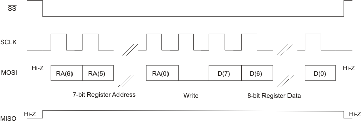
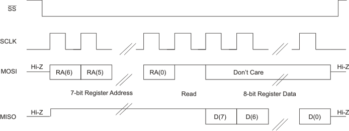
In the case of a register write, set the R/W bit to 0. A second byte of data is sent to the MOSI pin and contains the data to be written to the register. A register read is accomplished in a similar fashion. The 8-bit command word sends the 7-bit register address, followed by the R/W bit equal to 1 to signify a register read. The 8-bit register data is then clocked out of the device on the MISO pin during the second eight SCLK clocks in the frame. The device supports sequential SPI addressing for a multiple-byte data write/read transfer until the SSZ pin is pulled high. A multiple-byte data write or read transfer is identical to a single-byte data write or read transfer, respectively, until all data byte transfers complete. The host device must keep the SSZ pin low during all data byte transfers. Figure 93 shows the single-byte write transfer and Figure 94 shows the single-byte read transfer.
Table 1. SPI Command Word
| BIT 7 | BIT 6 | BIT 5 | BIT 4 | BIT 3 | BIT 2 | BIT 1 | BIT 0 |
|---|---|---|---|---|---|---|---|
| ADDR(6) | ADDR(5) | ADDR(4) | ADDR(3) | ADDR(2) | ADDR(1) | ADDR(0) | R/WZ |
 Figure 93. SPI Single-Byte Write Transfer
  Figure 94. SPI Single-Byte Read Transfer