JAJSMF1G April 2006 – July 2021 TLV320AIC3106
PRODUCTION DATA
- 1 特長
- 2 アプリケーション
- 3 概要
- 4 Revision History
- 5 概要 (続き)
- 6 Device Comparison Table
- 7 Pin Configuration and Functions
- 8 Specifications
- 9 Parameter Measurement Information
-
10Detailed Description
- 10.1 Overview
- 10.2 Functional Block Diagram
- 10.3
Feature Description
- 10.3.1 Hardware Reset
- 10.3.2 Digital Audio Data Serial Interface
- 10.3.3 Audio Data Converters
- 10.3.4 Audio Analog Inputs
- 10.3.5 Analog Fully Differential Line Output Drivers
- 10.3.6 Analog High Power Output Drivers
- 10.3.7 Input Impedance and VCM Control
- 10.3.8 General-Purpose I/O
- 10.3.9 Digital Microphone Connectivity
- 10.3.10 Micbias Generation
- 10.3.11 Short Circuit Output Protection
- 10.3.12 Jack/Headset Detection
- 10.4 Device Functional Modes
- 10.5 Programming
- 10.6 Register Maps
- 11Application and Implementation
- 12Power Supply Recommendations
- 13Layout
- 14Device and Documentation Support
パッケージ・オプション
デバイスごとのパッケージ図は、PDF版データシートをご参照ください。
メカニカル・データ(パッケージ|ピン)
- RGZ|48
- ZXH|80
サーマルパッド・メカニカル・データ
- RGZ|48
発注情報
10.3.4 Audio Analog Inputs
The TLV320AIC3106 includes ten analog audio input pins, which can be configured as up to four fully-differential pair plus one single-ended pair of audio inputs, or up to six single-ended audio inputs. . These pins connect through series resistors and switches to the virtual ground terminals of two fully differential opamps (one per ADC/PGA channel). By selecting to turn on only one set of switches per opamp at a time, the inputs can be effectively muxed to each ADC PGA channel.
By selecting to turn on multiple sets of switches per opamp at a time, mixing can also be achieved. Mixing of multiple inputs can easily lead to PGA outputs that exceed the range of the internal opamps, resulting in saturation and clipping of the mixed output signal. Whenever mixing is being implemented, the user should take adequate precautions to avoid such a saturation case from occurring. In general, the mixed signal should not exceed 2 Vpp (single-ended) or 4 Vpp (differential).
In most mixing applications, there is also a general need to adjust the levels of the individual signals being mixed. For example, if a soft signal and a large signal are to be mixed and played together, the soft signal generally should be amplified to a level comparable to the large signal before mixing. In order to accommodate this need, the TLV320AIC3106 includes input level control on each of the individual inputs before they are mixed or muxed into the ADC PGAs, with gain programmable from 0 dB to –12 dB in 1.5 dB steps. Note that this input level control is not intended to be a volume control, but instead used occasionally for level setting. Soft-stepping of the input level control settings is implemented in this device, with the speed and functionality following the settings used by the ADC PGA for soft-stepping.
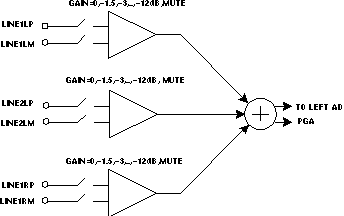
The TLV320AIC3106 supports the ability to mix up to three fully-differential analog inputs into each ADC PGA channel. Figure 10-12 shows the mixing configuration for the left channel, which can mix the signals LINE1LP-LINE1LM, LINE2LP-LINE2LM, and LINE1RP-LINE1RM.
 Figure 10-12 Left
Channel Fully-Differential Analog Input Mixing Configuration
Figure 10-12 Left
Channel Fully-Differential Analog Input Mixing ConfigurationThree fully-differential analog inputs can similarly be mixed into the right ADC PGA as well, consisting of LINE1RP-LINE1RM, LINE2RP-LINE2RM, and LINE1LP-LINE1LM. Note that it is not necessary to mix all three fully-differential signals if this is not desired – unnecessary inputs can simply be muted using the input level control registers.
Inputs can also be selected as single-ended instead of fully-differential, and mixing or muxing into the ADC PGAs is also possible in this mode. It is not possible, however, for an input pair to be selected as fully-differential for connection to one ADC PGA and simultaneously selected as single-ended for connection to the other ADC PGA channel. However, it is possible for an input to be selected or mixed into both left and right channel PGAs, as long as it has the same configuration for both channels (either both single-ended or both fully-differential).
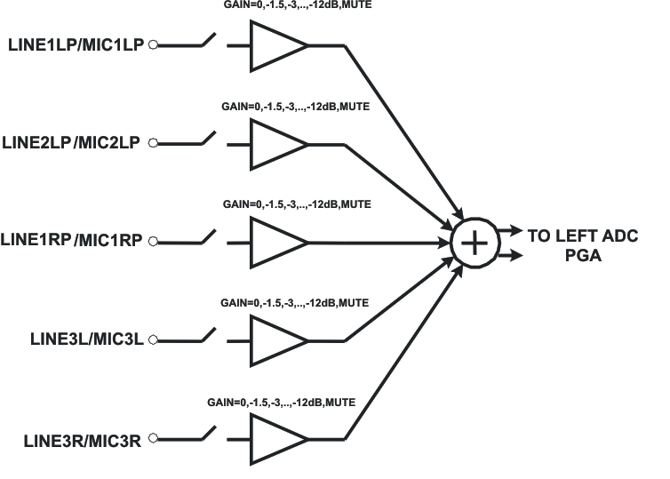
Figure 10-13 shows the single-ended mixing configuration for the left channel ADC PGA, which enables mixing of the signals LINE1LP, LINE2LP, LINE1RP, MIC3L, and MIC3R. The right channel ADC PGA mix is similar, enabling mixing of the signals LINE1RP, LINE2RP, LINE1LP, MIC3L, and MIC3R.
 Figure 10-13 Left
Channel Single-Ended Analog Input Mixing Configuration