JAJSMF1G April 2006 – July 2021 TLV320AIC3106
PRODUCTION DATA
- 1 特長
- 2 アプリケーション
- 3 概要
- 4 Revision History
- 5 概要 (続き)
- 6 Device Comparison Table
- 7 Pin Configuration and Functions
- 8 Specifications
- 9 Parameter Measurement Information
-
10Detailed Description
- 10.1 Overview
- 10.2 Functional Block Diagram
- 10.3
Feature Description
- 10.3.1 Hardware Reset
- 10.3.2 Digital Audio Data Serial Interface
- 10.3.3 Audio Data Converters
- 10.3.4 Audio Analog Inputs
- 10.3.5 Analog Fully Differential Line Output Drivers
- 10.3.6 Analog High Power Output Drivers
- 10.3.7 Input Impedance and VCM Control
- 10.3.8 General-Purpose I/O
- 10.3.9 Digital Microphone Connectivity
- 10.3.10 Micbias Generation
- 10.3.11 Short Circuit Output Protection
- 10.3.12 Jack/Headset Detection
- 10.4 Device Functional Modes
- 10.5 Programming
- 10.6 Register Maps
- 11Application and Implementation
- 12Power Supply Recommendations
- 13Layout
- 14Device and Documentation Support
パッケージ・オプション
デバイスごとのパッケージ図は、PDF版データシートをご参照ください。
メカニカル・データ(パッケージ|ピン)
- RGZ|48
- ZXH|80
サーマルパッド・メカニカル・データ
- RGZ|48
発注情報
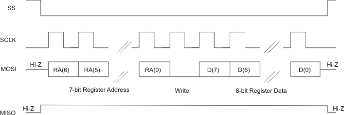
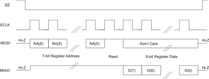
10.5.1.1 SPI Control Mode
 Figure 10-22 SPI Write
 Figure 10-23 SPI Read
In the SPI control mode, the TLV320AIC3106 uses the pins MFP0=SSB, MFP1=SCLK, MFP2=MISO, MFP3=MOSI as a standard SPI port with clock polarity setting of 0 (typical microprocessor SPI control bit CPOL = 0). The SPI port allows full-duplex, synchronous, serial communication between a host processor (the master) and peripheral devices (slaves). The SPI master (in this case, the host processor) generates the synchronizing clock (driven onto SCLK) and initiates transmissions. The SPI slave devices (such as the TLV320AIC3106) depend on a master to start and synchronize transmissions.
A transmission begins when initiated by an SPI master. The byte from the SPI master begins shifting in on the slave MOSI pin under the control of the master serial clock (driven onto SCLK). As the byte shifts in on the MOSI pin, a byte shifts out on the MISO pin to the master shift register.
The TLV320AIC3106 interface is designed so that with a clock phase bit setting of 1 (typical microprocessor SPI control bit CPHA = 1), the master begins driving its MOSI pin and the slave begins driving its MISO pin on the first serial clock edge. The SSB pin can remain low between transmissions; however, the TLV320AIC3106 only interprets the first 8 bits transmitted after the falling edge of SSB as a command byte, and the next 8 bits as a data byte only if writing to a register. Reserved register bits should be written to their default values.