JAJSHF9E September 2008 – September 2019 TLV320AIC3204
PRODUCTION DATA.
- 1 特長
- 2 アプリケーション
- 3 概要
- 4 改訂履歴
- 5 Device Comparison Table
- 6 Pin Configuration and Functions
-
7 Specifications
- 7.1 Absolute Maximum Ratings
- 7.2 ESD Ratings
- 7.3 Recommended Operating Conditions
- 7.4 Thermal Information
- 7.5 Electrical Characteristics, ADC
- 7.6 Electrical Characteristics, Bypass Outputs
- 7.7 Electrical Characteristics, Microphone Interface
- 7.8 Electrical Characteristics, Audio DAC Outputs
- 7.9 Electrical Characteristics, LDO
- 7.10 Electrical Characteristics, Misc.
- 7.11 Electrical Characteristics, Logic Levels
- 7.12 I2S LJF and RJF Timing in Master Mode (see )
- 7.13 I2S LJF and RJF Timing in Slave Mode (see )
- 7.14 DSP Timing in Master Mode (see )
- 7.15 DSP Timing in Slave Mode (see )
- 7.16 Digital Microphone PDM Timing (see )
- 7.17 I2C Interface Timing
- 7.18 SPI Interface Timing (See )
- 7.19 Typical Characteristics
- 7.20 Typical Characteristics, FFT
- 8 Parameter Measurement Information
- 9 Detailed Description
- 10Application and Implementation
- 11Power Supply Recommendations
- 12Layout
- 13デバイスおよびドキュメントのサポート
- 14メカニカル、パッケージ、および注文情報
パッケージ・オプション
メカニカル・データ(パッケージ|ピン)
- RHB|32
サーマルパッド・メカニカル・データ
- RHB|32
発注情報
7.20 Typical Characteristics, FFT
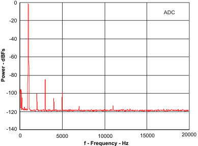 Figure 15. Single Ended Line Input to ADC FFT at -1dBr vs Frequency
 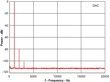 Figure 17. DAC Playback to Line-out FFT at -1dBFS vs Frequency
 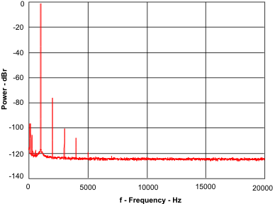 Figure 19. Line Input to Line-out FFT at 446mVrms vs Frequency
 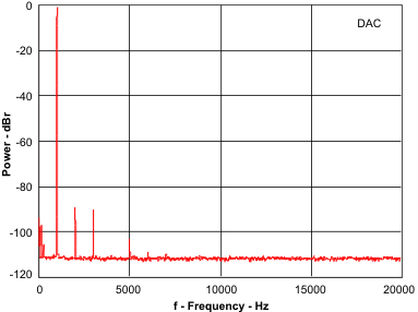 Figure 16. DAC Playback to Headphone FFT at -1dBFS vs Frequency
 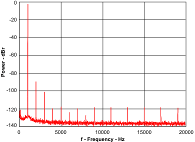 Figure 18. Line Input to Headphone FFT at 446mVrms vs Frequency