SLCS135B August 2000 – January 2017 TLV3401 , TLV3402 , TLV3404
PRODUCTION DATA.
- 1 Features
- 2 Applications
- 3 Description
- 4 Revision History
- 5 Device Comparison Table
- 6 Pin Configuration and Functions
- 7 Specifications
- 8 Detailed Description
- 9 Application and Implementation
- 10Power Supply Recommendations
- 11Layout
- 12Device and Documentation Support
- 13Mechanical, Packaging, and Orderable Information
パッケージ・オプション
メカニカル・データ(パッケージ|ピン)
サーマルパッド・メカニカル・データ
発注情報
1 Features
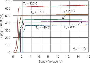
- Low Supply Current: 470 nA Per Channel
- Input Common-Mode Range Exceeds the Rails: –0.1 V to VCC + 5 V
- Supply Voltage Range: 2.5 V to 16 V
- Reverse Battery Protection Up to 18 V
- Open-Drain CMOS Output Stage
- Specified Temperature Range:
- Commercial Grade: 0°C to +70°C
- Industrial Grade: –40°C to +125°C
- Ultra-Small Packaging:
- 5-Pin SOT-23 (TLV3401)
- 8-Pin MSOP (TLV3402)
- Universal Op Amp EVM (See Universal Operational Amplifier Evaluation Module Selection Guide For More Information)
2 Applications
- Portable Medical Equipment
- Wireless Security Systems
- Remote Control Systems
- Handheld Instruments
- Ultra-Low Power Systems
Supply Current vs Supply Voltage

3 Description
The TLV340x is TI's first family of nanopower comparators with only 470 nA per channel supply current, which makes this device ideal for battery-powered and wireless handset applications.
The TLV340x has a minimum operating supply voltage of 2.7 V over the extended industrial temperature range (TA = –40°C to +125°C), while having an input common-mode range of –0.1 to
VCC + 5 V. The low supply current makes it an ideal choice for battery-powered portable applications where quiescent current is the primary concern. Reverse battery protection guards the amplifier from an overcurrent condition due to improper battery installation. For harsh environments, the inputs can be taken 5 V above the positive supply rail without damage to the device.
All members are available in PDIP and SOIC with the single versions in the small SOT-23 package, dual versions in the VSSOP package, and quad versions in the TSSOP package.
Device Information(1)
| PART NUMBER | PACKAGE | BODY SIZE (NOM) |
|---|---|---|
| TLV3401 | SOT-23 (5) | 2.90 mm × 1.60 mm |
| TLV3401, TLV3402 | SOIC (8) | 4.90 mm × 3.91 mm |
| TLV3401, TLV3402 | PDIP (8) | 9.81 mm × 6.35 mm |
| TLV3402 | VSSOP (8) | 3.00 mm × 3.00 mm |
| TLV3404 | SOIC (14) | 8.65 mm × 3.91 mm |
| TSSOP (14) | 5.00 mm × 4.40 mm | |
| PDIP (14) | 19.30 mm × 6.35 mm |
- For all available packages, see the orderable addendum at the end of the data sheet.
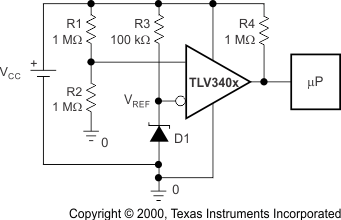
High-Side Voltage Sense Circuit

4 Revision History
Changes from A Revision (November 2000) to B Revision
- Added ESD Rating table, Feature Description section, Device Functional Modes, Application and Implementation section, Power Supply Recommendations section, Layout section, Device and Documentation Support section, and Mechanical, Packaging, and Orderable Information section; Go
- Deleted Available Options tables; refer to Package Option Addendum at the end of this data sheetGo
- Deleted Dissipation Ratings tableGo