JAJSOI5B June 2023 – September 2024 TLV2365-Q1 , TLV365-Q1
PRODMIX
- 1
- 1 特長
- 2 アプリケーション
- 3 概要
- 4 Device Comparison Table
- 5 Pin Configuration and Functions
- 6 Specifications
- 7 Detailed Description
- 8 Application and Implementation
- 9 Device and Documentation Support
- 10Revision History
- 11Mechanical, Packaging, and Orderable Information
パッケージ・オプション
デバイスごとのパッケージ図は、PDF版データシートをご参照ください。
メカニカル・データ(パッケージ|ピン)
- DBV|5
サーマルパッド・メカニカル・データ
発注情報
8.1.2 Achieving an Output Level of Zero Volts
Certain single-supply applications require the op‑amp output to swing from 0 V to a positive full-scale voltage and have high accuracy. An example is an op amp employed to drive a single-supply ADC having an input range from 0 V to 3.3 V. Rail-to-rail output amplifiers with very light output loading can achieve an output level within few millivolts of 0 V (or V+ at the high end), but not true 0 V. Furthermore, the deviation from 0 V only becomes greater as the required load current increases. This increased deviation is a result of limitations of the CMOS output stage.
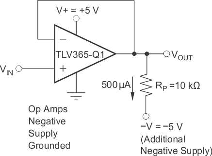
When a pulldown resistor is connected from the amplifier output to a negative voltage source, the TLVx365-Q1 can achieve an output level of 0 V, and even a few millivolts below 0 V. Figure 8-3 shows a circuit using this technique.
 Figure 8-3 Swing-to-Ground
A pulldown current of approximately 500 μA is required when TLVx365-Q1 is connected as a unity-gain buffer. Pulldown resistor RL is calculated from RL = [(VO − VNEG) / (500 μA)].
Figure 8-4 shows the offset voltage vs output swing.

| VS = ±2.75 V |