SLVSBC1D October 2013 – October 2016 TLV62565 , TLV62566
PRODUCTION DATA.
- 1 Features
- 2 Applications
- 3 Description
- 4 Simplified Schematic
- 5 Revision History
- 6 Device Comparison Table
- 7 Pin Configuration and Functions
- 8 Specifications
- 9 Detailed Description
- 10Application and Implementation
- 11Power Supply Recommendations
- 12Layout
- 13Device and Documentation Support
- 14Mechanical, Packaging, and Orderable Information
10 Application and Implementation
NOTE
Information in the following applications sections is not part of the TI component specification, and TI does not warrant its accuracy or completeness. TI’s customers are responsible for determining suitability of components for their purposes. Customers should validate and test their design implementation to confirm system functionality.
10.1 Application Information
The TLV6256x devices are synchronous step-down converters optimized for small solution size and high efficiency. The devices integrate switches capable of delivering an output current up to 1.5 A.
10.2 Typical Application
TLV62565 2.7-V to 5.5-V input, 1.2-V output converter.
 Figure 8. TLV62565 1.2-V Output Application
Table 1. List of Components
| REFERENCE | DESCRIPTION | MANUFACTURER |
|---|---|---|
| C1 | 4.7 µF, Ceramic Capacitor, 6.3 V, X5R, size 0603, GRM188R60J475ME84 | Murata |
| C2 | 10 µF, Ceramic Capacitor, 6.3 V, X5R, size 0603, GRM188R60J106ME84 | Murata |
| L1 | 2.2 µH, Power Inductor, 2.5 A, size 4mmx4mm, LQH44PN2R2MP0 | Murata |
| R1, R2 | Chip resistor,1%,size 0603 | Std. |
10.2.1 Design Requirements
10.2.1.1 Output Filter Design
The inductor and output capacitor together provide a low-pass frequency filter. To simplify this process, Table 2 outlines possible inductor and capacitor value combinations.
Table 2. Matrix of Output Capacitor and Inductor Combinations
| L [µH](1) | COUT [µF](2) (3) | ||||
|---|---|---|---|---|---|
| 4.7 | 10 | 22 | 47 | 100 | |
| 1 | |||||
| 2.2 | + (4) | +(4) | + | ||
| 4.7 | |||||
10.2.1.2 Inductor Selection
The main parameters for inductor selection is inductor value and then saturation current of the inductor. To calculate the maximum inductor current under static load conditions, Equation 1 is given:
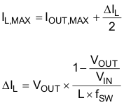
where
- IOUT,MAX is the maximum output current
- ΔIL is the inductor current ripple
- fSW is the switching frequency
- L is the inductor value
It is recommended to choose a saturation current for the inductor that is approximately 20% to 30% higher than IL,MAX. In addition, DC resistance and size should also be taken into account when selecting an appropriate inductor. The recommended inductors are listed in Table 3.
Table 3. List of Recommended Inductors
| INDUCTANCE [µH] |
CURRENT RATING [mA] |
DIMENSIONS L x W x H [mm3] |
DC RESISTANCE [mΩ typ] |
TYPE | MANUFACTURER |
|---|---|---|---|---|---|
| 2.2 | 2500 | 4 x 3.7 x 1.65 | 49 | LQH44PN2R2MP0 | Murata |
| 2.2 | 3000 | 4 x 4 x 1.8 | 50 | NRS4018T2R2MDGJ | Taiyo Yuden |
10.2.1.3 Input and Output Capacitor Selection
The input capacitor is the low impedance energy source for the converter that helps provide stable operation. The closer the input capacitor is placed to the VIN and GND pins, the lower the switch ring. A low ESR multilayer ceramic capacitor is recommended for best filtering. For most applications, 4.7-µF input capacitance is sufficient; a larger value reduces input voltage ripple.
The architecture of the TLV62565/6 allow use of tiny ceramic-type output capacitors with low equivalent series resistance (ESR). These capacitors provide low output voltage ripple and are thus recommended. To keep its resistance up to high frequencies and to achieve narrow capacitance variation with temperature, it is recommended to use X7R or X5R dielectric. The TLV62565/6 are designed to operate with an output capacitance of 10 µF to 47 µF, as outlined in Table 2.
10.2.2 Detailed Design Procedure
10.2.2.1 Setting the Output Voltage
An external resistor divider is used to set output voltage. By selecting R1 and R2, the output voltage is programmed to the desired value. When the output voltage is regulated, the typical voltage at the FB pin is VFB. Equation 2, Equation 3, and Equation 4 can be used to calculate R1 and R2.
When sizing R2, in order to achieve low current consumption and acceptable noise sensitivity, use a minimum of 5 μA for the feedback current IFB. Larger currents through R2 improve noise sensitivity and output voltage accuracy but increase current consumption.


Due to the maximum duty cycle limit, the output voltage is out of regulation if the input voltage is too low. For proper regulation, VOUT should be set below VIN_MIN as shown in Equation 5.
10.2.2.2 Loop Stability
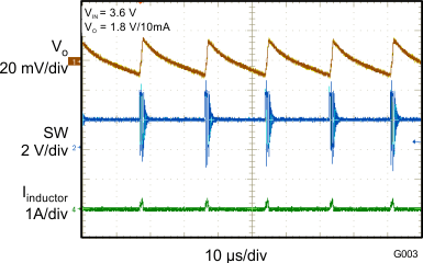
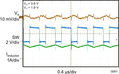
The first step of circuit and stability evaluation is to look from a steady-state perspective at the following signals:
- Switching node, SW
- Inductor current, IL
- Output ripple voltage, VOUT(AC)
These are the basic signals that need to be measured when evaluating a switching converter. When the switching waveform shows large duty cycle jitter or the output voltage or inductor current shows oscillations, the regulation loop may be unstable. This is often a result of board layout and/or L-C combination. Applications with the recommended L-C combinations in Table 2 are designed for good loop stability as well as fast load transient response.
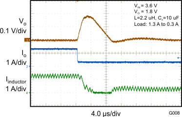
As a next step in the evaluation of the regulation loop, the load transient response is illustrated. The TLV62565/6 use a constant on time with valley current mode control, so the on time of the high-side MOSFET is relatively consistent from cycle to cycle when a load transient occurs. Whereas the off time adjusts dynamically in accordance with the instantaneous load change and brings VOUT back to the regulated value.
During recovery time, VOUT can be monitored for settling time, overshoot, or ringing which helps judge the stability of the converter. Without any ringing, the loop usually has more than 45° of phase margin.
10.2.3 Application Performance Curves

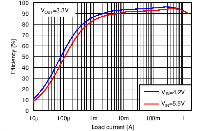
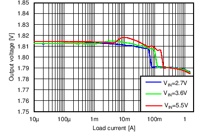
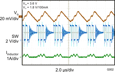
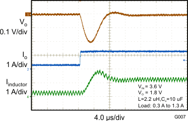
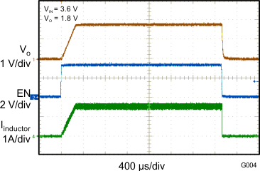
| IOUT = 1.5 A | ||
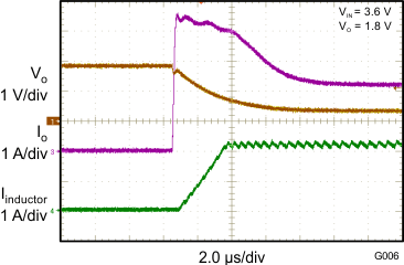
| No load to short circuit | ||
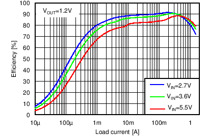
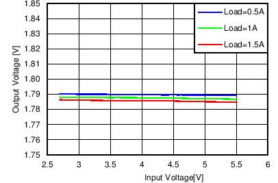
| IOUT = 1.5 A | ||
