JAJSEJ9B January   2018  – October 2018 TLV6710

PRODUCTION DATA.  

  1. 特長
  2. アプリケーション
  3. 概要
    1.     Device Images
      1.      ブロック概略図
  4. 改訂履歴
  5. デバイス比較表
  6. Pin Configuration and Functions
    1.     Pin Functions
  7. Specifications
    1. 7.1 Absolute Maximum Ratings
    2. 7.2 ESD Ratings
    3. 7.3 Recommended Operating Conditions
    4. 7.4 Thermal Information
    5. 7.5 Electrical Characteristics
    6. 7.6 Timing Requirements
    7. 7.7 Typical Characteristics
  8. Detailed Description
    1. 8.1 Overview
    2. 8.2 Functional Block Diagram
    3. 8.3 Feature Description
      1. 8.3.1 Inputs (INA, INB)
      2. 8.3.2 Outputs (OUTA, OUTB)
    4. 8.4 Device Functional Modes
      1. 8.4.1 Normal Operation (VDD > UVLO)
      2. 8.4.2 Undervoltage Lockout (V(POR) < VDD < UVLO)
      3. 8.4.3 Power On Reset (VDD < V(POR))
  9. Application and Implementation
    1. 9.1 Application Information
      1. 9.1.1 Window Comparator Considerations
      2. 9.1.2 Input and Output Configurations
      3. 9.1.3 Immunity to Input Pin Voltage Transients
    2. 9.2 Typical Application
      1. 9.2.1 Design Requirements
      2. 9.2.2 Detailed Design Procedure
      3. 9.2.3 Application Curve
    3. 9.3 Do's and Don'ts
  10. 10Power Supply Recommendations
  11. 11Layout
    1. 11.1 Layout Guidelines
    2. 11.2 Layout Example
  12. 12デバイスおよびドキュメントのサポート
    1. 12.1 デバイス・サポート
      1. 12.1.1 開発サポート
    2. 12.2 ドキュメントのサポート
      1. 12.2.1 関連資料
    3. 12.3 ドキュメントの更新通知を受け取る方法
    4. 12.4 コミュニティ・リソース
    5. 12.5 商標
    6. 12.6 静電気放電に関する注意事項
    7. 12.7 Glossary
  13. 13メカニカル、パッケージ、および注文情報

パッケージ・オプション

メカニカル・データ(パッケージ|ピン)
サーマルパッド・メカニカル・データ
発注情報

Power Supply Recommendations

The TLV6710 has a 40-V absolute maximum rating on the VDD pin, with a recommended operating condition of 36 V. If the voltage supply that is providing power to VDD is susceptible to any large voltage transient that may exceed 40 V, or if the supply exhibits high voltage slew rates greater than 1 V/µs, take additional precautions. Place an RC filter between the supply and VDD to filter any high-frequency transient surges on the VDD pin. A 100-Ω resistor and 0.01-µF capacitor is required in these cases, as shown in Figure 26.
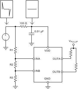
TLV6710 vdd_filter_snvsav4.gifFigure 26. Using an RC Filter to Remove High-Frequency Disturbances on VDD