SLVSA00E September   2009  – April 2015 TLV700

PRODUCTION DATA.  

  1. Features
  2. Applications
  3. Description
  4. Revision History
  5. Pin Configuration and Functions
  6. Specifications
    1. 6.1 Absolute Maximum Ratings
    2. 6.2 ESD Ratings
    3. 6.3 Recommended Operating Conditions
    4. 6.4 Thermal Information
    5. 6.5 Electrical Characteristics
    6. 6.6 Typical Characteristics
  7. Detailed Description
    1. 7.1 Overview
    2. 7.2 Functional Block Diagram
    3. 7.3 Feature Description
      1. 7.3.1 Internal Current Limit
      2. 7.3.2 Shutdown
      3. 7.3.3 Dropout Voltage
      4. 7.3.4 Undervoltage Lockout (UVLO)
    4. 7.4 Device Functional Modes
      1. 7.4.1 Normal Operation
      2. 7.4.2 Dropout Operation
  8. Application and Implementation
    1. 8.1 Application Information
    2. 8.2 Typical Application
      1. 8.2.1 Design Requirements
      2. 8.2.2 Detailed Design Procedure
        1. 8.2.2.1 Input and Output Capacitor Requirements
        2. 8.2.2.2 Transient Response
      3. 8.2.3 Application Curves
  9. Power Supply Recommendations
  10. 10Layout
    1. 10.1 Layout Guidelines
    2. 10.2 Layout Examples
    3. 10.3 Thermal Protection
    4. 10.4 Power Dissipation
  11. 11Device and Documentation Support
    1. 11.1 Device Support
      1. 11.1.1 Development Support
        1. 11.1.1.1 Evaluation Modules
        2. 11.1.1.2 Spice Models
      2. 11.1.2 Device Nomenclature
    2. 11.2 Documentation Support
      1. 11.2.1 Related Documentation
    3. 11.3 Trademarks
    4. 11.4 Electrostatic Discharge Caution
    5. 11.5 Glossary
  12. 12Mechanical, Packaging, and Orderable Information

パッケージ・オプション

メカニカル・データ(パッケージ|ピン)
サーマルパッド・メカニカル・データ

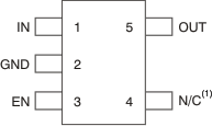
5 Pin Configuration and Functions

DSE Package
6-Pin WSON
Top View
TLV700 po_dse_lvsa00.gif
DCK Package
5-Pin SC70
Top View
TLV700 po_dck_lvsa00.gif
DDC Package
5-Pin SOT
Top View
TLV700 po_ddc_lvsa00.gif
1. No connection.

Pin Functions

PIN I/O DESCRIPTION
NAME WSON SC70 SOT
IN 1 1 1 I Input pin. A small, 1-μF ceramic capacitor is recommended from this pin to ground to assure stability and good transient performance. See for more details.
GND 2 2 2 Ground pin
EN 6 3 3 I Enable pin. Driving EN over 0.9 V turns on the regulator. Driving EN below 0.4 V puts the regulator into shutdown mode and reduces operating current to 1 μA, nominal.
NC 4, 5 4 4 No connection. This pin can be tied to ground to improve thermal dissipation.
OUT 3 5 5 O Regulated output voltage pin. A small, 1-μF ceramic capacitor is needed from this pin to ground to assure stability. See for more details.