SLVSB67C November   2011  – June 2017 TLV70012-Q1 , TLV70018-Q1

PRODUCTION DATA.  

  1. Features
  2. Applications
  3. Description
  4. Revision History
  5. Pin Configuration and Functions
  6. Specifications
    1. 6.1 Absolute Maximum Ratings
    2. 6.2 ESD Ratings
    3. 6.3 Recommended Operating Conditions
    4. 6.4 Thermal Information
    5. 6.5 Electrical Characteristics
    6. 6.6 Typical Characteristics
  7. Detailed Description
    1. 7.1 Overview
    2. 7.2 Functional Block Diagrams
    3. 7.3 Feature Description
      1. 7.3.1 Internal Current Limit
      2. 7.3.2 Dropout Voltage
      3. 7.3.3 Undervoltage Lockout (UVLO)
      4. 7.3.4 Thermal Shutdown
    4. 7.4 Device Functional Modes
      1. 7.4.1 Shutdown
      2. 7.4.2 Operation with VIN Less than 2 V
      3. 7.4.3 Operation with VIN Greater than 2 V
  8. Application and Implementation
    1. 8.1 Application Information
    2. 8.2 Typical Application
      1. 8.2.1 Design Requirements
      2. 8.2.2 Detailed Design Procedure
        1. 8.2.2.1 Input and Output Capacitor Requirements
        2. 8.2.2.2 Transient Response
      3. 8.2.3 Application Curve
  9. Power Supply Recommendations
  10. 10Layout
    1. 10.1 Layout Guidelines
    2. 10.2 Layout Example
    3. 10.3 Thermal Considerations
    4. 10.4 Power Dissipation
      1. 10.4.1 Thermal Calculations
  11. 11Device and Documentation Support
    1. 11.1 Device Support
      1. 11.1.1 Package Mounting
    2. 11.2 Documentation Support
      1. 11.2.1 Related Documentation
    3. 11.3 Related Links
    4. 11.4 Receiving Notification of Documentation Updates
    5. 11.5 Community Resources
    6. 11.6 Trademarks
    7. 11.7 Electrostatic Discharge Caution
    8. 11.8 Glossary
  12. 12Mechanical, Packaging, and Orderable Information

パッケージ・オプション

メカニカル・データ(パッケージ|ピン)
サーマルパッド・メカニカル・データ
発注情報

Pin Configuration and Functions

DDC Package
5-Pin SOT
Top View
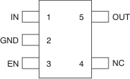
TLV70018-Q1 TLV70012-Q1 po_dbv_lvsag6.gif

Pin Functions

PIN DESCRIPTION
NO. NAME
1 IN Input pin. A small 1-μF ceramic capacitor is recommended from this pin to ground to assure stability and good transient performance.(1)
2 GND Ground pin
3 EN Enable pin. Driving EN over 0.9 V turns on the regulator. Driving EN below 0.4 V puts the regulator into shutdown mode and reduces operating current to 1 μA, nominal.
4 NC No connection. This pin can be tied to ground to improve thermal dissipation.
5 OUT Regulated output voltage pin. A small 1-μF ceramic capacitor is needed from this pin to ground to assure stability.(1)
See Input and Output Capacitor Requirements section for more details.