-
TLV705 200-mA, Low IQ, Low-Noise, Low-Dropout Regulator in Ultra-Small, 0.77-mm × 0.77-mm DSBGA and PicoStar
- 1 Features
- 2 Applications
- 3 Description
- 4 Revision History
- 5 Pin Configuration and Functions
- 6 Specifications
- 7 Detailed Description
- 8 Application and Implementation
- 9 Power Supply Recommendations
- 10Layout
- 11Device and Documentation Support
- 12Mechanical, Packaging, and Orderable Information
- IMPORTANT NOTICE
TLV705 200-mA, Low IQ, Low-Noise, Low-Dropout Regulator in Ultra-Small, 0.77-mm × 0.77-mm DSBGA and PicoStar
1 Features
-
Very Low Dropout:
- 105 mV at IOUT = 150 mA
- 145 mV at IOUT = 200 mA
- Accuracy: 0.5% Typical
- Low IQ: 35 μA
- Available in Fixed-Output Voltages From
0.7 V to 4.8 V - VIN Range: 2 V to 5.5 V
- High PSRR: 70 dB at 1 kHz
- Stable With Effective Capacitance of 0.1 μF
- Thermal Shutdown and Overcurrent Protection
- Available in an Ultra-Low Profile (0.15-mm Maximum Height) PicoStar Package Option
2 Applications
3 Description
The TLV705 series of low-dropout (LDO) linear regulators are low quiescent current devices with excellent line and load transient performance. These devices are designed for power-sensitive applications, with a precision band gap. An error amplifier provides typical accuracy of 0.5%. Low output noise, very high power-supply rejection ratio (PSRR), and low dropout voltage make this series of LDOs ideal for a wide selection of battery-operated handheld equipment. All devices have a thermal shutdown and current limit for safety.
Furthermore, the TLV705 series is stable with an effective output capacitance of only 0.1 μF. This feature enables the use of cost-effective capacitors that have higher bias voltage and temperature derating. The devices regulate to the specified accuracy with zero output load. The TLV705P series also provides an active pulldown circuit to quickly discharge output.
The TLV705 and TLV705P series are both available in 0.77-mm × 0.77-mm DSBGA and PicoStar packages with three height options that are optimal for handheld applications.
Device Information(1)
| PART NUMBER | PACKAGE | BODY SIZE (NOM) |
|---|---|---|
| TLV705 | DSGBA (4) | 0.77 mm × 0.77 mm |
| PicoStar (4) | 0.77 mm × 0.77 mm |
- For all available packages, see the orderable addendum at the end of the data sheet.
4 Revision History
Changes from E Revision (May 2015) to F Revision
- Deleted "x" from TLV705 device in document title Go
- Changed package dimensions in document title from "0.8-mm × 0.8-mm" to "0.77-mm × 0.77-mm" Go
- Changed ultra-low profile maximum height from 0.2-mm to 0.15-mm in Applications section Go
- Changed package dimensions in Description section from 0.8-mm to 0.77-mm.Go
- Changed DSBGA package dimensions from "0.80 mm × 0.80 mm" to "0.77 mm × 0.77 mm" in the Device Information table Go
- Added copyright statement to the Typical Application Circuit Go
- Changed formatting of Thermal Information table note Go
- Deleted "x" from device number in Thermal Information table Go
- Added copyright statement to functional block diagrams in Functional Block Diagrams section Go
- Added copyright statement to Typical Application Circuit (Fixed-Voltage Versions) in the Typical Application section Go
- Changed formatting of document reference in Related Documentation section Go
- Changed table header title from "Sample & Buy" to "Order Now" in the Related Links table Go
Changes from D Revision (April 2015) to E Revision
- Added new package (YFM) to document Go
- Added PicoStar to title Go
- Changed last Features bullet Go
- Changed last sentence of Description section Go
- Added second row to Device Information table Go
- Added YFM pin out drawingGo
- Added YFM package to Thermal Information table Go
- Changed VO parameter units in Electrical Characteristics table: % for first row, mV for second rowGo
- Changed first sentence of Overview section: removed new Go
- Changed fifth sentence of Internal Current Limit section to clarify description of the shutdown circuit functionality Go
- Changed Vµs to V/µs in second paragraph of Start-Up Current section Go
- Changed it to the start-up current in third paragraph of Start-Up Current section Go
- Changed INPUT to VIN in Power Supply Recommendations section Go
- Added Related Links section Go
- Added YFM package to Package Mounting section Go
Changes from C Revision (October 2012) to D Revision
- Added ESD Ratings table, Feature Description section, Device Functional Modes, Application and Implementation section, Power Supply Recommendations section, Layout section, Device and Documentation Support section, and Mechanical, Packaging, and Orderable Information section Go
- Added Features bullet for VIN range Go
- Changed Applications list items Go
- Deleted Power Dissipation Ratings table Go
- Changed y-axis unit measurement from ILIM to ICL for Figure 11Go
- Changed Figure 31 and deleted layout silkscreen images; replaced with image of PCB layout drawing.Go
- Changed title for Figure 31 Go
- Changed title of Thermal Protection section Go
Changes from B Revision (December 2011) to C Revision
- Deleted last Features bulletGo
Changes from A Revision (August 2011) to B Revision
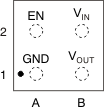
5 Pin Configuration and Functions
Pin Functions
| PIN | I/O | DESCRIPTION | |
|---|---|---|---|
| NAME | NO. | ||
| GND | A1 | — | Ground pin. |
| EN | A2 | I | Enable pin. Driving EN over 0.9 V turns on the regulator. Driving EN below 0.4 V places the regulator into shutdown mode, which reduces the operating current to 1 μA (nominal). |
| VOUT | B1 | O | Regulated output voltage pin. Placing a small 1-μF ceramic capacitor is required from this pin to ground to ensure stability. See Input and Output Capacitor Requirements for more details. |
| VIN | B2 | I | Input pin. TI recommends placing a small 1-µF capacitor from this pin to ground for good transient performance. See Input and Output Capacitor Requirements for more details. |
6 Specifications
6.1 Absolute Maximum Ratings
specified at TJ = –40°C to +125°C, unless otherwise noted. All voltages are with respect to GND.(1)| MIN | MAX | UNIT | ||
|---|---|---|---|---|
| Voltage(2) | VIN | –0.3 | 6 | V |
| VEN | –0.3 | 6 | V | |
| VOUT | –0.3 | 6 | V | |
| Maximum output current | IOUT | Internally limited | ||
| Output short-circuit duration | Indefinite | |||
| Temperature | Operating junction, TJ | –55 | 150 | °C |
| Storage, Tstg | –55 | 150 | °C | |
6.2 ESD Ratings
| VALUE | UNIT | |||
|---|---|---|---|---|
| V(ESD) | Electrostatic discharge | Human body model (HBM), per ANSI/ESDA/JEDEC JS-001(1) | ±2000 | V |
| Charged device model (CDM), per JEDEC specification JESD22-C101(2) | ±500 | |||
6.3 Recommended Operating Conditions
over operating junction temperature range (unless otherwise noted)| MIN | NOM | MAX | UNIT | ||
|---|---|---|---|---|---|
| VIN | Input voltage | 2 | 5.5 | V | |
| VOUT | Output voltage | 0.7 | 4.8 | V | |
| IOUT | Output current | 0 | 200 | mA | |
| TJ | Junction temperature | –40 | 125 | °C | |
6.4 Thermal Information
| THERMAL METRIC(1) | TLV705 | UNIT | ||
|---|---|---|---|---|
| YFF, YFP (DSBGA) |
YFM (PicoStar) |
|||
| 4 PINS | 4 PINS | |||
| RθJA | Junction-to-ambient thermal resistance | 160 | 191.7 | °C/W |
| RθJC(top) | Junction-to-case (top) thermal resistance | 80 | 3.1 | °C/W |
| RθJB | Junction-to-board thermal resistance | 90 | 36.5 | °C/W |
| ψJT | Junction-to-top characterization parameter | 0.5 | 2.8 | °C/W |
| ψJB | Junction-to-board characterization parameter | 78 | 26.5 | °C/W |
6.5 Electrical Characteristics
at TJ = –40°C to +125°C, VIN = VOUT(nom) + 0.5 V or 2 V (whichever is greater), IOUT = 10 mA, VEN = 0.9 V, andCOUT = 1 μF, unless otherwise noted. Typical values are at TJ = 25°C.
| PARAMETER | TEST CONDITIONS | MIN | TYP | MAX | UNIT | ||
|---|---|---|---|---|---|---|---|
| VIN | Input voltage range | 2 | 5.5 | V | |||
| VOUT | Output voltage range | 0.7 | 4.8 | V | |||
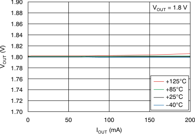
| VO | DC output accuracy | –40°C ≤ TJ ≤ 125°C | 0 mA ≤ IOUT ≤ 200 mA, VOUT ≥ 1 V | –2% | ±0.5% | 2% | |
| 0 mA ≤ IOUT ≤ 200 mA, VOUT < 1 V | –20 | ±5 | 20 | mV | |||
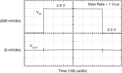
| ΔVOUT(ΔVIN) | Line regulation | VOUT(nom) + 0.5 V ≤ VIN ≤ 5.5 V | 0.05 | 5 | mV | ||
| ΔVOUT(ΔIOUT) | Load regulation | 0 mA ≤ IOUT ≤ 200 mA | 1 | mV | |||
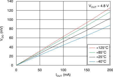
| VDO | Dropout voltage(1) | VIN = 0.98 × VOUT(nom), IOUT = 200 mA | 145 | 250 | mV | ||
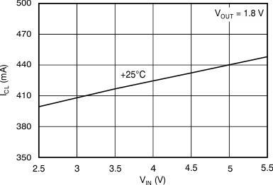
| ICL | Output current limit | VOUT = 0.9 × VOUT(nom), TJ = 25°C | 260 | 400 | 550 | mA | |
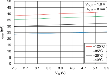
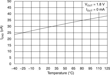
| IGND | Ground pin current | IOUT = 0 mA | 35 | 55 | μA | ||
| IOUT = 200 mA | 315 | μA | |||||
| ISHUTDOWN | Shutdown ground pin current | VEN ≤ 0.4 V, 2 V ≤ VIN ≤ 4.5 V | 1 | 1.8 | μA | ||
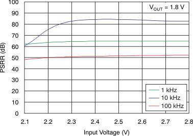
| PSRR | Power-supply rejection ratio | VIN = 2.3 V, VOUT = 1.8 V, IOUT = 10 mA, f = 10 kHz |
80 | dB | |||
| VIN = 2.3 V, VOUT = 1.8 V, IOUT = 10 mA, f = 1 MHz |
55 | dB | |||||
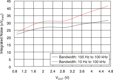
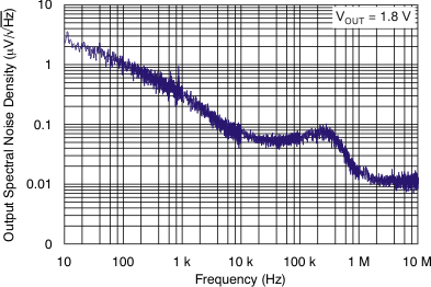
| Vn | Output noise voltage | BW = 100 Hz to 100 kHz, IOUT = 10 mA |
VIN = 2.3 V, VOUT = 1.8 V | 26.6 | μVRMS | ||
| VIN = 3.3 V, VOUT = 2.8 V | 26.7 | μVRMS | |||||
| VIN = 3.8 V, VOUT = 3.3 V | 28.2 | μVRMS | |||||
| BW = 10 Hz to 100 kHz, IOUT = 10 mA | VIN = 2.3 V, VOUT = 1.8 V | 30.7 | μVRMS | ||||
| VIN = 3.3 V, VOUT = 2.8 V | 31.3 | μVRMS | |||||
| VIN = 3.8 V, VOUT = 3.3 V | 34.1 | μVRMS | |||||
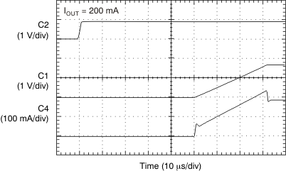
| tSTR | Start-up time(2) | COUT = 1 μF, IOUT = 200 mA | 100 | μs | |||
| VHI | Enable high (enabled) | 0.9 | VIN | V | |||
| VLO | Enable low (disabled) | 0 | 0.4 | V | |||
| IEN | EN pin current | VEN = 5.5 V | 0.01 | μA | |||
| UVLO | Undervoltage lockout | VIN rising | 1.9 | V | |||
| tSD | Thermal shutdown temperature | Shutdown, temperature increasing | 160 | °C | |||
| Reset, temperature decreasing | 140 | °C | |||||
| TJ | Operating junction temperature | –40 | 125 | °C | |||
6.6 Typical Characteristics
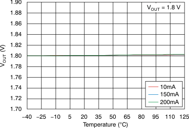
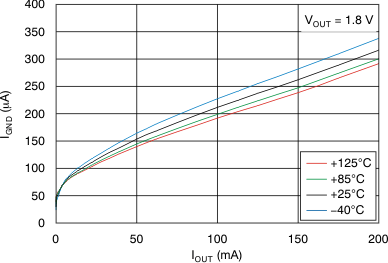
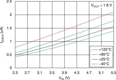
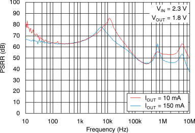
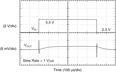
over operating temperature range (TJ = –40°C to +125°C), IOUT = 10 mA, VEN = 0.9 V, COUT = 1 μF, and VIN = VOUT(nom) + 0.5 V or 2 V, whichever is greater, unless otherwise noted. Typical values are at TJ = 25°C.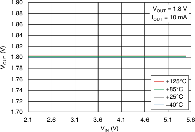
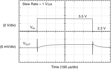
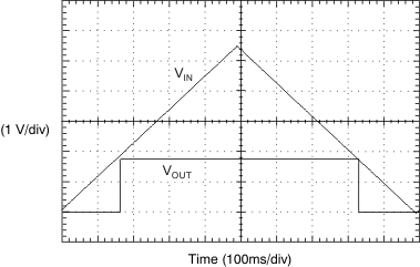
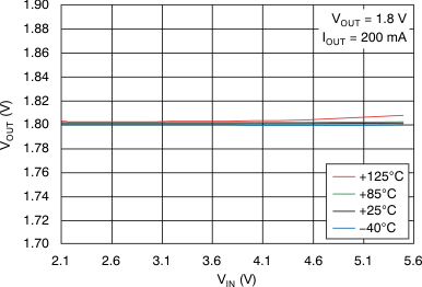
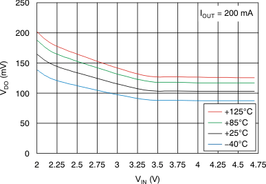

7 Detailed Description
7.1 Overview
The TLV705 and TLV705P series of devices belong to a family of next-generation value low-dropout (LDO) voltage regulators. These devices consume low quiescent current and deliver excellent line and load transient performance. This performance, combined with low noise, very good PSRR with little (VIN – VOUT) headroom, makes these devices ideal for RF portable applications. This family of regulators offers sub-band-gap output voltages down to 0.7 V, current limit, and thermal protection, and are specified from –40°C to +125°C. The TLV705P provides an active pulldown circuit to quickly discharge the outputs.
7.3 Feature Description
7.3.1 Internal Current Limit
The internal current limits of the TLV705 series help protect the regulator during fault conditions. During current limit, the output sources a fixed amount of current that is largely independent of output voltage. In such a case, the output voltage is not regulated, and can be measured as VOUT = ILIMIT × RLOAD. The PMOS pass transistor dissipates [(VIN – VOUT) × ILIMIT] until a thermal shutdown is triggered and the device turns off. When the device cools down, the internal thermal shutdown circuit turns the device back on. If the fault condition continues, the device cycles between current limit and thermal shutdown; see Power Dissipation and Junction Temperature for more details.
The PMOS pass element in the TLV705 has a built-in body diode that conducts current when the voltage at VOUT exceeds the voltage at VIN. This current is not limited, so if extended reverse voltage operation is anticipated, TI recommends external limiting to 5% of the rated output current.
7.3.2 Undervoltage Lockout (UVLO)
The TLV705 uses an UVLO circuit to keep the output shut off until the internal circuitry is operating properly.
7.3.3 Start-Up Current
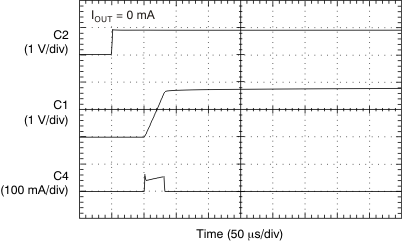
The TLV705 uses a unique start-up architecture that creates a constant start-up time regardless of the output capacitor. The start-up current is given by Equation 1. Equation 1 shows that start-up current is directly proportional to COUT.
The output voltage ramp rate is independent of COUT and the load current, and has a typical value of 0.06 V/μs.
The TLV705 automatically adjusts the soft-start current to supply both the load current and the current to charge COUT. For example, if ILOAD = 0 mA upon enabling the LDO, then ISTARTUP = 1 μF × 0.06 Vμs + 0 mA = 60 mA, which is the current that charges the output capacitor.
However, if ILOAD = 200 mA, then ISTARTUP = 1 μF × 0.06 V / μs + 200 mA = 260 mA, which is the required current to charge the output capacitor and supply the load current.
If the output capacitor and load increase such that the start-up current exceeds the output current limit, the start-up current is clamped at the typical current limit of 400 mA. For example, if COUT = 10 μF and
IOUT = 200 mA, then 10 μF × 0.06 V / μs + 200 mA = 800 mA is not supplied and is instead clamped at 400 mA.
7.3.4 Dropout Voltage
The TLV705 uses a PMOS pass transistor to achieve low dropout. When (VIN – VOUT) is less than the dropout voltage (VDO), the PMOS pass device is in the linear region of operation and the input-to-output resistance is the RDS(on) of the PMOS pass element. VDO approximately scales with the output current because the PMOS device functions as a resistor in dropout.
As with any linear regulator, PSRR and transient response are degraded as (VIN – VOUT) approaches dropout. This effect is shown in Figure 13 in the Typical Characteristics.
7.3.5 Shutdown
The enable pin (EN) is active high. The device is enabled when the EN pin goes above 0.9 V. This relatively lower value of voltage required to turn the LDO on can power the device with the GPIO of recent processors with a GPIO voltage lower than traditional microcontrollers. The device is turned off when the EN pin is held at less than 0.4 V. When shutdown capability is not required, EN can be connected to the VIN pin. The TLV705P version has internal active pulldown circuitry that discharges the output with a time constant of:
where
- RL = load resistance
- COUT = output capacitor
7.4 Device Functional Modes
7.4.1 Normal Operation
The device regulates to the nominal output voltage under the following conditions:
- The input voltage is greater than the nominal output voltage added to the dropout voltage.
- The output current is less than the current limit.
- The input voltage is greater than the UVLO voltage.
7.4.2 Dropout Operation
If the input voltage is lower than the nominal output voltage plus the specified dropout voltage, but all other conditions are met for normal operation, the device operates in dropout mode. In this condition, the output voltage is the same the input voltage minus the dropout voltage. The transient performance of the device is significantly degraded because the pass device is in a triode state and no longer regulates the output voltage of the LDO. Line or load transients in dropout can result in large output voltage deviations.
Table 1 lists the conditions that lead to the different modes of operation.
Table 1. Device Functional Mode Comparison
| OPERATING MODE | PARAMETER | |
|---|---|---|
| VIN | IOUT | |
| Normal mode | VIN > VOUT (nom) + VDO | IOUT < ICL |
| Dropout mode | VIN < VOUT (nom) + VDO | IOUT < ICL |
| Current limit | VIN > UVLO | IOUT > ICL |
8 Application and Implementation
NOTE
Information in the following applications sections is not part of the TI component specification, and TI does not warrant its accuracy or completeness. TI’s customers are responsible for determining suitability of components for their purposes. Customers should validate and test their design implementation to confirm system functionality.
8.1 Application Information
The TLV705 is a LDO that offers very low dropout voltages in a tiny package. The operating junction temperature of this device is –40°C to +125°C.
8.2 Typical Application
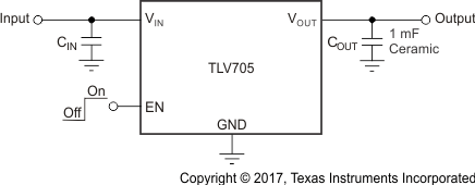 Figure 28. Typical Application Circuit (Fixed-Voltage Versions)
8.2.1 Design Requirements
Table 2 lists the design parameters.
Table 2. Design Parameters
| PARAMETER | DESIGN REQUIREMENT |
|---|---|
| Input voltage | 2.5 V to 3.3 V |
| Output voltage | 1.8 V |
| Output current | 100 mA |
8.2.2 Detailed Design Procedure
Select the desired device based on the output voltage.
Provide an input supply with adequate headroom to account for dropout. The input supply must also provide adequate current to account for the GND pin current and load current.
8.2.2.1 Input and Output Capacitor Requirements
TI recommends using 1-μF X5R- and X7R-type ceramic capacitors because these components have minimal variation in value and equivalent series resistance (ESR) over temperature. However, the TLV705 series is designed to be stable with an effective capacitance of 0.1 μF or larger at the output. As a result, the device is stable with capacitors of other dielectrics as long as the effective capacitance under the operating bias voltage and temperature is greater than 0.1 μF. This effective capacitance refers to the capacitance that the LDO detects under operating bias voltage and temperature conditions (that is, the capacitance after taking the bias voltage and temperature derating into consideration). In addition to allowing the use of lower cost dielectrics, the effective capacitance enables using smaller footprint capacitors that have higher derating in space-constrained applications.
Using a 0.1-μF rating capacitor at the output of the LDO does not ensure stability because the effective capacitance under operating conditions is less than 0.1 μF. Maximum ESR must be less than 200 mΩ.
Although an input capacitor is not required for stability, good analog design practice is to connect a 0.1-μF to
1-μF low ESR capacitor across the VIN and GND pins of the regulator. This capacitor counteracts reactive input sources and improves transient response, noise rejection, and ripple rejection. A higher-value capacitor can be necessary if large, fast rise-time load transients are anticipated, or if the device is not located close to the power source. If source impedance is more than 2 Ω, a 0.1-μF input capacitor may be necessary to ensure stability.
8.2.2.2 Transient Response
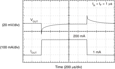
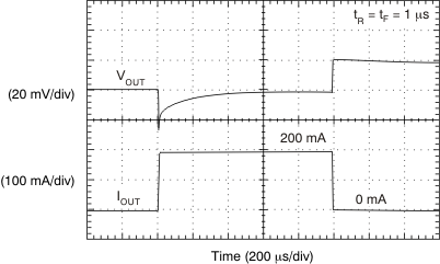
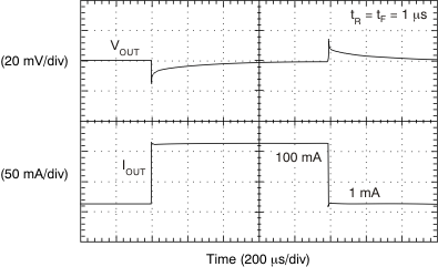
As with any regulator, increasing the size of the output capacitor reduces overshoot and undershoot magnitude, but increases the duration of the transient response.
8.2.3 Application Curves


8.3 Do's and Don'ts
Place input and output capacitors as close as possible to the device.
Do not exceed the device absolute maximum ratings.
