SBVS266 May 2015 TLV713P-Q1
PRODUCTION DATA.
1 Features
- AEC-Q100 Qualified with the Following Results:
- Device Temperature Grade 1: –40°C to 125°C Ambient Operating Temperature Range
- Device HBM ESD Classification Level H2
- Device CDM ESD Classification Level C4B
- Input Voltage Range: 1.4 V to 5.5 V
- Stable Operation With or Without Capacitors
- Foldback Overcurrent Protection
- Package: 5-Pin SOT-23
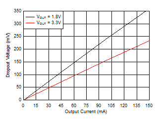
- Very Low Dropout: 230 mV at 150 mA
- Accuracy: 1%
- Low IQ: 50 µA
- Available in Fixed-Output Voltages:
- 1 V to 3.3 V
- High PSRR: 65 dB at 1 kHz
- Active Output Discharge
2 Applications
- Automotive Head Units
- Audio Amplifiers
- DI Clusters
- ADAS ECUs
- Microprocessor Rails
- USBs
- Body Electronics
3 Description
The TLV713P-Q1 series of low-dropout (LDO) linear regulators are low quiescent current LDOs with excellent line and load transient performance and are designed for power-sensitive applications. These devices provide a typical accuracy of 1%.
The TLV713P-Q1 series of devices is designed to be stable without an output capacitor. The removal of the output capacitor allows for a very small solution size. However, the TLV713P-Q1 series is also stable with any output capacitor if an output capacitor is used.
The TLV713P-Q1 also provides inrush current control during device power-up and enabling. The TLV713P-Q1 limits the input current to the defined current limit to avoid large currents from flowing from the input power source. This functionality is especially important in battery-operated devices.
The TLV713P-Q1 series is available in a standard DBV package and provides an active pulldown circuit to quickly discharge output loads. The TLV713P-Q1 is suited for automotive applications because the device is qualified for AEC-Q100 grade 1.
Device Information(1)
| PART NUMBER | PACKAGE | BODY SIZE (NOM) |
|---|---|---|
| TLV713P-Q1 | SOT-23 (5) | 2.90 mm × 1.60 mm |
- For all available packages, see the orderable addendum at the end of the data sheet.
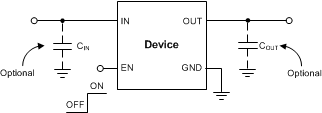
Typical Application Circuit

Dropout Voltage vs Output Current
