SBVS217B June 2013 – November 2015 TLV716P
PRODUCTION DATA.
- 1 Features
- 2 Applications
- 3 Description
- 4 Revision History
- 5 Pin Configuration and Functions
- 6 Specifications
- 7 Detailed Description
- 8 Application and Implementation
- 9 Power Supply Recommendations
- 10Layout
- 11Device and Documentation Support
- 12Mechanical, Packaging, and Orderable Information
パッケージ・オプション
メカニカル・データ(パッケージ|ピン)
- DPQ|6
サーマルパッド・メカニカル・データ
- DPQ|6
発注情報
10 Layout
10.1 Layout Guidelines
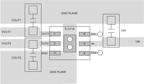
If used, place the input and output capacitors as close to the device pins as possible. To maximize AC performance refer to Figure 27.
10.2 Layout Example
 Figure 27. Layout Recommendation
10.3 Thermal Considerations
Thermal protection disables the output when the junction temperature rises to approximately 158°C, allowing the device to cool. When the junction temperature cools to approximately 140°C, the output circuitry is again enabled. Depending on power dissipation, thermal resistance, and ambient temperature, the thermal protection circuit may cycle on and off. This cycling limits the dissipation of the regulator, protecting it from damage as a result of overheating.
Any tendency to activate the thermal protection circuit indicates excessive power dissipation or an inadequate heatsink. For reliable operation, junction temperature should be limited to 125°C maximum. To estimate the margin of safety in a complete design, increase the ambient temperature until the thermal protection is triggered; use worst-case loads and signal conditions. The ambient temperature at which thermal shutdown occurs on the device is 33°C higher (158°C - 125°C) than the maximum recommended operating conditions.
The internal protection circuitry of the TLV716 and TLV716P is designed to protect against overload conditions. This circuitry is not intended to replace proper PCB layout and heatsinking. Continuously running the device into thermal shutdown degrades reliability.
10.4 Power Dissipation
The ability to remove heat from a die is different for each package type, presenting different considerations in the printed-circuit-board (PCB) layout. The copper PCB area around the device that is free of other components moves the heat from the device to ambient air. Performance data for JEDEC high-K boards are given in the Thermal Information table. Using heavier copper increases effectiveness in removing heat from the device.
Power dissipation (PD) is equal to the product of the output current and the voltage drop across both output pass elements, as shown in Equation 1:
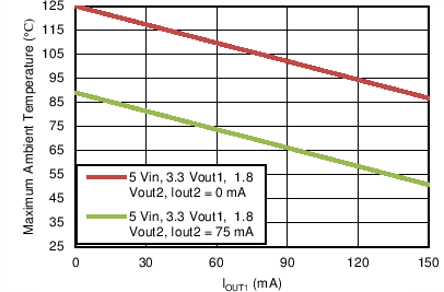
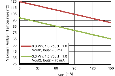
The maximum ambient temperature that the device can operate within the maximum TJ operating temperature of 125°C depends on the thermal impedance and the total power dissipated within the device. Figure 28 and Figure 29 show maximum ambient temperature verses output current for two different LDO configurations. Figure 29 shows the maximum ambient temperature with VIN = 3.3 V, VOUT1 = 1.8 V, and VOUT2 = 1 V versus IOUT1. Figure 28 shows the maximum ambient temperature with VIN = 5 V, VOUT1 = 3.3 V, and VOUT2 = 1.8 V versus IOUT1.
 Figure 28. Maximum Ambient Temperature vs Output Current
(VIN = 5 V, VOUT1 = 3.3 V, VOUT2 = 1.8 V)
 Figure 29. Maximum Ambient Temperature vs Output Current
(VIN = 3.3 V, VOUT1 = 1.8 V, VOUT2 = 1 V)