JAJSHL1J August 2018 – May 2021 TLV803E , TLV809E , TLV810E
PRODMIX
- 1 特長
- 2 アプリケーション
- 3 概要
- 4 Revision History
- 5 Device Comparison
- 6 Pin Configuration and Functions
- 7 Specifications
- 8 Detailed Description
- 9 Application and Implementation
- 10Power Supply Recommendations
- 11Layout
- 12Device and Documentation Support
- 13Mechanical, Packaging, and Orderable Information
パッケージ・オプション
メカニカル・データ(パッケージ|ピン)
サーマルパッド・メカニカル・データ
- DPW|5
発注情報
6 Pin Configuration and Functions
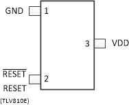
 Figure 6-1 DBZ Package
 (Pin 1 = GND)
3-Pin SOT-23
Top View
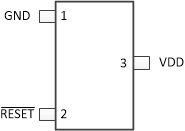
 Figure 6-2 DCK Package
3-Pin SC-70
Top View
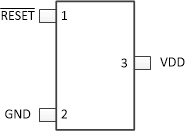
 Figure 6-3 DBZ Package
 (Pin 1 = RESET, R pinout)
3-Pin SOT-23
Top View
Figure 6-5 DPW Package
5-Pin X2SON
See Table 6-1
Top View
5-Pin X2SON
See Table 6-1
Top View
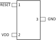
 Figure 6-4 DBZ Package
 (Pin 3 = GND, V pinout)
3-Pin SOT-23
Top View
Table 6-1 Pin Functions
| PIN | I/O | DESCRIPTION | ||||
|---|---|---|---|---|---|---|
| NAME | DCK, DBZ | DBZ (V PINOUT) |
DBZ (R PINOUT) |
DPW | ||
| GND | 1 | 3 | 2 | 4 | — | Ground |
| RESET | 2 | 1 | 1 | 1 | O | Active-low output reset signal: This pin is driven low logic when VDD voltage falls below the negative voltage threshold (VIT–). RESET remains low (asserted) for the delay time period (tD) after VDD voltage rise above VIT+. |
| RESET | 2 | 1 | 1 | 1 | O | Active-High output reset signal (TLV810E only): This pin is driven high logic when VDD voltage falls below the negative voltage threshold (VIT–). RESET remains high (asserted) for the delay time period (tD) after VDD voltage rise above VIT+. |
| VDD | 3 | 2 | 3 | 5 | I | Input supply voltage. TLV803E, TLV809E, TLV810E monitor VDD voltage. |
| MR | N/A | N/A | N/A | 2 | I | Active-low manual reset input. Pull this pin to a logic low (VMR_L) to assert a reset signal in the output pin. After the MR pin is left floating or pulled to VMR_H the output goes to the nominal state after the reset delay time (tD) expires. MR can be left floating when not in use. |
| PAD | N/A | N/A | N/A | 3 | — | No Connection. Thermal pad helps with thermal dissipation. PAD does not need to be soldered down. PAD can be connected to GND. |