JAJSD06E December   2016  – April 2018 TLV8541 , TLV8542 , TLV8544

UNLESS OTHERWISE NOTED, this document contains PRODUCTION DATA.  

  1. 特長
  2. アプリケーション
  3. 概要
    1.     Device Images
      1.      低消費電力PIRモーション検出器
  4. 改訂履歴
  5. 概要(続き)
  6. Pin Configuration and Functions
    1.     Pin Functions: TLV8541 DBV
    2.     Pin Functions: TLV8542 D & RUG
    3.     Pin Functions: TLV8544 PW & D
  7. Specifications
    1. 7.1 Absolute Maximum Ratings
    2. 7.2 ESD Ratings
    3. 7.3 Recommended Operating Conditions
    4. 7.4 Thermal Information
    5. 7.5 Electrical Characteristics
    6. 7.6 Typical Characteristics
  8. Detailed Description
    1. 8.1 Overview
    2. 8.2 Functional Block Diagram
    3. 8.3 Feature Description
    4. 8.4 Device Functional Modes
      1. 8.4.1 Rail-To-Rail Input
      2. 8.4.2 Supply Current Changes Over Common Mode
      3. 8.4.3 Design Optimization With Rail-To-Rail Input
      4. 8.4.4 Design Optimization for Nanopower Operation
      5. 8.4.5 Common-Mode Rejection
      6. 8.4.6 Output Stage
      7. 8.4.7 Driving Capacitive Load
  9. Application and Implementation
    1. 9.1 Application Information
    2. 9.2 Typical Application: Battery-Powered Wireless PIR Motion Detectors
      1. 9.2.1 Design Requirements
      2. 9.2.2 Detailed Design Procedure
        1. 9.2.2.1 Calculation of the Cutoff Frequencies and Gain of Stage A:
        2. 9.2.2.2 Calculation of the Cutoff Frequencies and Gain of Stage B
        3. 9.2.2.3 Calculation of the Total Gain of Stages A and B
        4. 9.2.2.4 Window Comparator Stage
        5. 9.2.2.5 Reference Voltages
      3. 9.2.3 Application Curve
    3. 9.3 Typical Application: 60-Hz Twin T Notch Filter
      1. 9.3.1 Design Requirements
      2. 9.3.2 Detailed Design Procedure
      3. 9.3.3 Application Curve
    4. 9.4 Dos and Don'ts
  10. 10Power Supply Recommendations
  11. 11Layout
    1. 11.1 Layout Guidelines
    2. 11.2 Layout Example
  12. 12デバイスおよびドキュメントのサポート
    1. 12.1 デバイス・サポート
      1. 12.1.1 開発サポート
    2. 12.2 ドキュメントのサポート
      1. 12.2.1 関連資料
    3. 12.3 関連リンク
    4. 12.4 ドキュメントの更新通知を受け取る方法
    5. 12.5 コミュニティ・リソース
    6. 12.6 商標
    7. 12.7 静電気放電に関する注意事項
    8. 12.8 Glossary
  13. 13メカニカル、パッケージ、および注文情報

パッケージ・オプション

メカニカル・データ(パッケージ|ピン)
サーマルパッド・メカニカル・データ
発注情報

Supply Current Changes Over Common Mode

Because of the ultra-low supply current, changes in common mode voltages cause a noticeable change in the supply current as the input stages transition through the transition region, as shown in Figure 30.
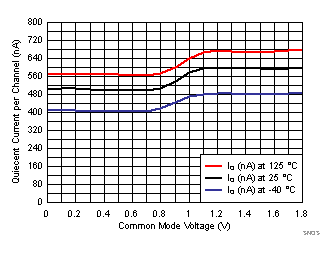
TLV8544 TLV8542 TLV8541 SNOSD29_IQ_Vs_Vcm_1p8V_3Temp.gifFigure 30. Supply Current Change Over Common Mode at 1.8 V

For the lowest supply current operation, keep the input common mode range between V– and 1 V below V+.