JAJSUS9A June   2024  – August 2024 TLV9044-Q1

PRODMIX  

  1.   1
  2. 特長
  3. アプリケーション
  4. 概要
  5. Pin Configuration and Functions
  6. Specifications
    1. 5.1 Absolute Maximum Ratings
    2. 5.2 ESD Ratings
    3. 5.3 Recommended Operating Conditions
    4. 5.4 Thermal Information for Quad Channel
    5. 5.5 Electrical Characteristics
    6. 5.6 Typical Characteristics
  7. Detailed Description
    1. 6.1 Overview
    2. 6.2 Functional Block Diagram
    3. 6.3 Feature Description
      1. 6.3.1 Operating Voltage
      2. 6.3.2 Rail-to-Rail Input
      3. 6.3.3 Rail-to-Rail Output
      4. 6.3.4 Common-Mode Rejection Ratio (CMRR)
      5. 6.3.5 Capacitive Load and Stability
      6. 6.3.6 Overload Recovery
      7. 6.3.7 EMI Rejection
      8. 6.3.8 Electrical Overstress
      9. 6.3.9 Input and ESD Protection
    4. 6.4 Device Functional Modes
  8. Application and Implementation
    1. 7.1 Application Information
    2. 7.2 Typical Application
      1. 7.2.1 TLV904x-Q1 Low-Side, Current Sensing Application
        1. 7.2.1.1 Design Requirements
        2. 7.2.1.2 Detailed Design Procedure
        3. 7.2.1.3 Application Curve
    3. 7.3 Power Supply Recommendations
    4. 7.4 Layout
      1. 7.4.1 Layout Guidelines
      2. 7.4.2 Layout Example
  9. Device and Documentation Support
    1. 8.1 Documentation Support
      1. 8.1.1 Related Documentation
    2. 8.2 ドキュメントの更新通知を受け取る方法
    3. 8.3 サポート・リソース
    4.     Trademarks
    5. 8.4 静電気放電に関する注意事項
    6. 8.5 用語集
  10. Revision History
  11. 10Mechanical, Packaging, and Orderable Information

パッケージ・オプション

メカニカル・データ(パッケージ|ピン)
サーマルパッド・メカニカル・データ
発注情報

Typical Characteristics

at TA = 25°C, V+ = 2.75V, V– = –2.75V, RL = 10kΩ connected to VS / 2, VCM = VS / 2, and VOUT = VS / 2 (unless otherwise noted)
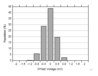
TLV9044-Q1 Offset Voltage Distribution Histogram
VS = 5.5V
Figure 5-1 Offset Voltage Distribution Histogram
TLV9044-Q1 Input
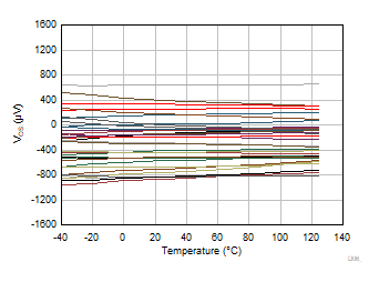
                        Offset Voltage vs Temperature
VS = 5.5V, VCM = V–
Figure 5-3 Input Offset Voltage vs Temperature
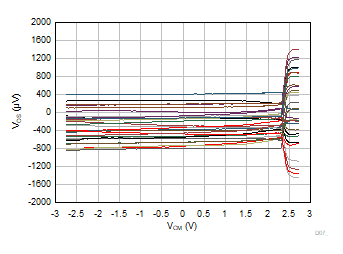
TLV9044-Q1 Offset Voltage vs Common-Mode
 
Figure 5-5 Offset Voltage vs Common-Mode
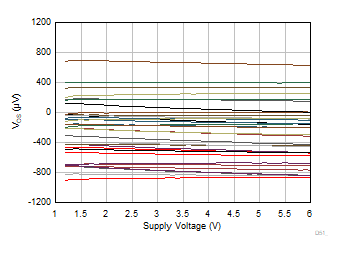
TLV9044-Q1 Offset Voltage vs Supply Voltage
VCM = (V–)
Figure 5-7 Offset Voltage vs Supply Voltage
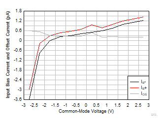
TLV9044-Q1 IB and IOS vs Common-Mode Voltage
Figure 5-9 IB and IOS vs Common-Mode Voltage
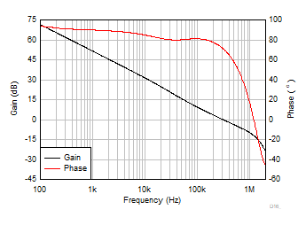
TLV9044-Q1 Open-Loop Gain and Phase vs Frequency
CL = 10pF
Figure 5-11 Open-Loop Gain and Phase vs Frequency
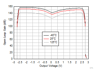
TLV9044-Q1 Open-Loop Gain vs Output Voltage
V+ = 2.75V, V– = –2.75VRL = 10kΩ
Figure 5-13 Open-Loop Gain vs Output Voltage
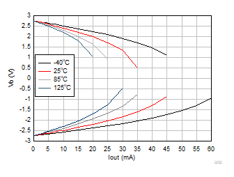
TLV9044-Q1 Output Voltage vs Output Current (Claw)
V+ = 2.75V, V– = –2.75V
Figure 5-15 Output Voltage vs Output Current (Claw)
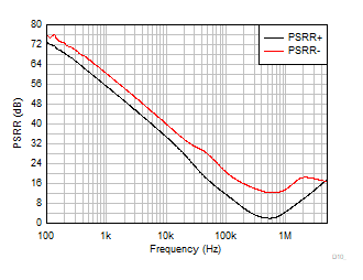
TLV9044-Q1 PSRR
                        vs Frequency
 
Figure 5-17 PSRR vs Frequency
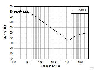
TLV9044-Q1 CMRR
                        vs Frequency
Figure 5-19 CMRR vs Frequency
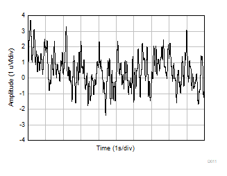
TLV9044-Q1 0.1Hz to 10Hz Voltage
                        Noise in Time Domain
Figure 5-21 0.1Hz to 10Hz Voltage Noise in Time Domain
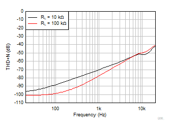
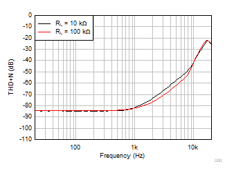
TLV9044-Q1 THD +
                        N vs Frequency
VS = 5.5VVCM = 2.5VG = 1
BW = 80kHzVOUT = 0.5VRMS
Figure 5-23 THD + N vs Frequency
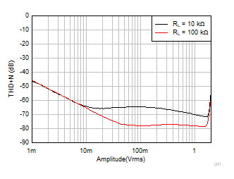
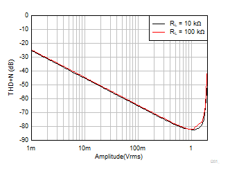
TLV9044-Q1 THD +
                        N vs Amplitude
VS = 5.5VVCM = 2.5Vf = 1kHz
G = 1BW = 80kHz
Figure 5-25 THD + N vs Amplitude
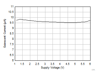
TLV9044-Q1 Quiescent Current vs Supply Voltage
Figure 5-27 Quiescent Current vs Supply Voltage
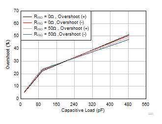
TLV9044-Q1 Small
                        Signal Overshoot vs Capacitive Load
G = 1VIN = 100mVpp
Figure 5-29 Small Signal Overshoot vs Capacitive Load
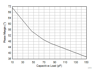
TLV9044-Q1 Phase
                        Margin vs Capacitive Load
 
Figure 5-31 Phase Margin vs Capacitive Load
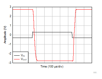
TLV9044-Q1 Overload Recovery
G = –10VIN = 600mVPP
Figure 5-33 Overload Recovery
TLV9044-Q1 Large-Signal Step Response
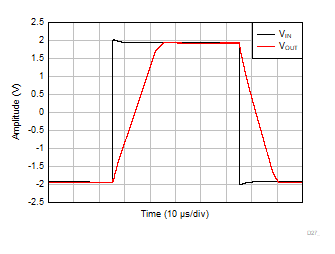
G = 1VIN = 4VPPCL = 10pF
Figure 5-35 Large-Signal Step Response
TLV9044-Q1 Large-Signal Settling Time (Positive)
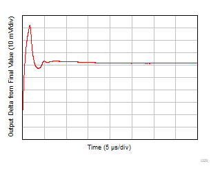
G = 1VIN = 4VPPCL = 10pF
Figure 5-37 Large-Signal Settling Time (Positive)
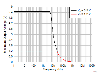
TLV9044-Q1 Maximum Output Voltage vs Frequency
Figure 5-39 Maximum Output Voltage vs Frequency
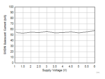
TLV9044-Q1 Shutdown Mode Quiescent Current vs Supply Voltage
Figure 5-41 Shutdown Mode Quiescent Current vs Supply Voltage
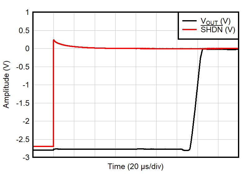
TLV9044-Q1 Amplifier Enable Response
Figure 5-43 Amplifier Enable Response
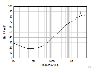
TLV9044-Q1 Electromagnetic Interference Rejection Ratio Referred to Noninverting Input
                        (EMIRR+) vs Frequency
Figure 5-45 Electromagnetic Interference Rejection Ratio Referred to Noninverting Input (EMIRR+) vs Frequency
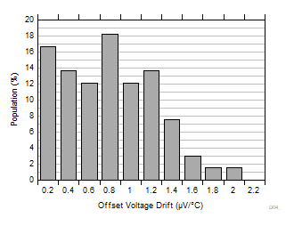
TLV9044-Q1 Offset Voltage Drift Distribution Histogram
VS = 5.5V, TA = –40°C to +125°C
Figure 5-2 Offset Voltage Drift Distribution Histogram
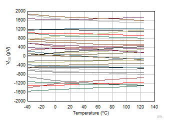
TLV9044-Q1 Input
                        Offset Voltage vs Temperature
VS = 5.5V, VCM = V+
Figure 5-4 Input Offset Voltage vs Temperature
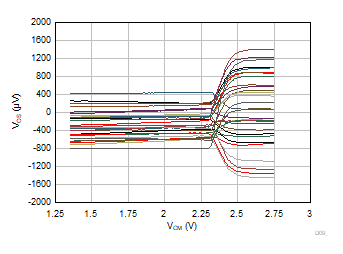
TLV9044-Q1 Offset Voltage vs Common-Mode
VCM > (V+) – 1.4V
Figure 5-6 Offset Voltage vs Common-Mode
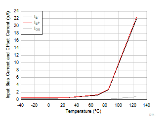
TLV9044-Q1 IB and IOS vs Temperature
 
Figure 5-8 IB and IOS vs Temperature
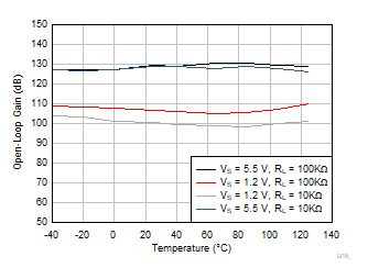
TLV9044-Q1 Open-Loop Gain vs Temperature
Figure 5-10 Open-Loop Gain vs Temperature
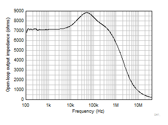
TLV9044-Q1 Open-Loop Output Impedance vs Frequency
 
Figure 5-12 Open-Loop Output Impedance vs Frequency
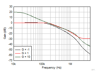
TLV9044-Q1 Closed-Loop Gain vs Frequency
CL = 10pF
Figure 5-14 Closed-Loop Gain vs Frequency
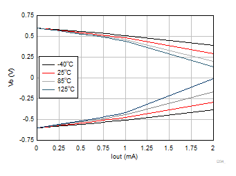
TLV9044-Q1 Output Voltage vs Output Current (Claw)
V+ = 0.6V, V– = –0.6V
Figure 5-16 Output Voltage vs Output Current (Claw)
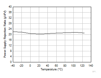
TLV9044-Q1 DC
                        PSRR vs Temperature
VS = 1.2V to 5.5V
Figure 5-18 DC PSRR vs Temperature
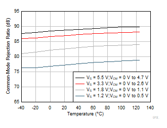
TLV9044-Q1 DC
                        CMRR vs Temperature
Figure 5-20 DC CMRR vs Temperature
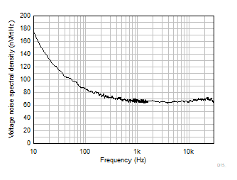
TLV9044-Q1 Input
                        Voltage Noise Spectral Density
Figure 5-22 Input Voltage Noise Spectral Density
TLV9044-Q1 THD +
                        N vs Frequency
VS = 5.5VVCM = 2.5VG = –1
BW = 80kHzVOUT = 0.5VRMS
Figure 5-24 THD + N vs Frequency
TLV9044-Q1 THD +
                        N vs Amplitude
VS = 5.5VVCM = 2.5Vf = 1kHz
G = –1BW = 80kHz
Figure 5-26 THD + N vs Amplitude
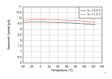
TLV9044-Q1 Quiescent Current vs Temperature
Figure 5-28 Quiescent Current vs Temperature
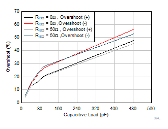
TLV9044-Q1 Small
                        Signal Overshoot vs Capacitive Load
G = –1VIN = 100mVpp
Figure 5-30 Small Signal Overshoot vs Capacitive Load
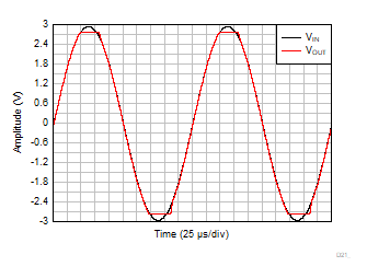
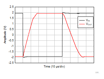
TLV9044-Q1 No
                        Phase Reversal
G = 1VIN = 6VPP
Figure 5-32 No Phase Reversal
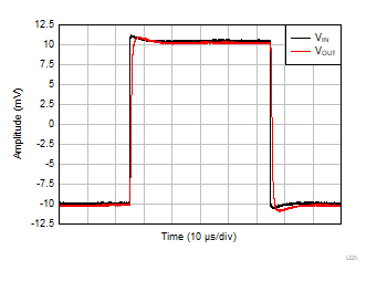
TLV9044-Q1 Small-Signal Step Response
G = 1VIN = 20mVPPCL = 10pF
Figure 5-34 Small-Signal Step Response
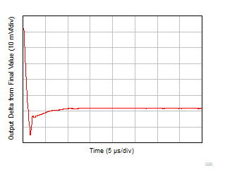
TLV9044-Q1 Large-Signal Settling Time (Negative)
G = 1VIN = 4VPPCL = 10pF
Figure 5-36 Large-Signal Settling Time (Negative)
TLV9044-Q1 Large-Signal Step Response
G = –1VIN = 4VPPCL = 10pF
Figure 5-38 Large-Signal Step Response
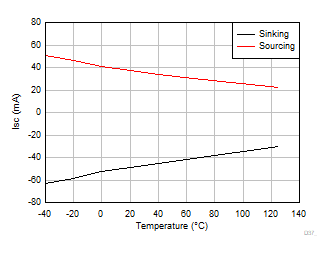
TLV9044-Q1 Short-Circuit Current vs Temperature
Figure 5-40 Short-Circuit Current vs Temperature
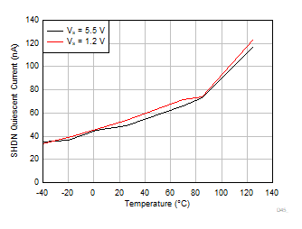
TLV9044-Q1 Shutdown Mode Quiescent Current vs Temperature
Figure 5-42 Shutdown Mode Quiescent Current vs Temperature
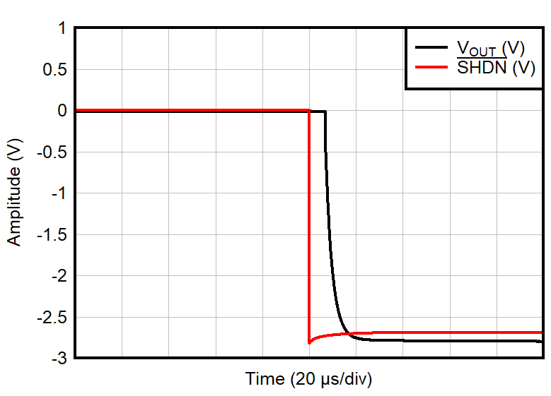
TLV9044-Q1 Amplifier Disable Response
Figure 5-44 Amplifier Disable Response
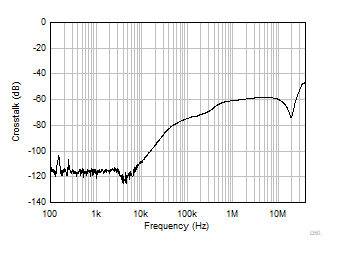
TLV9044-Q1 Channel Separation
Figure 5-46 Channel Separation