JAJSVW1
December 2024
TLV9141
,
TLV9144
PRODUCTION DATA
1
1
特長
2
アプリケーション
3
概要
4
Pin Configuration and Functions
5
Specifications
5.1
Absolute Maximum Ratings
5.2
ESD Ratings
5.3
Recommended Operating Conditions
5.4
Thermal Information for Single Channel
5.5
Thermal Information for Dual Channel
5.6
Thermal Information for Quad Channel
5.7
Electrical Characteristics
5.8
Typical Characteristics
6
Detailed Description
6.1
Overview
6.2
Functional Block Diagram
6.3
Feature Description
6.3.1
Input Protection Circuitry
6.3.2
Common-Mode Voltage Range
6.3.3
EMI Rejection
6.3.4
Phase Reversal Protection
6.3.5
Electrical Overstress
6.3.6
Overload Recovery
6.3.7
Typical Specifications and Distributions
6.4
Device Functional Modes
7
Application and Implementation
7.1
Application Information
7.2
Typical Applications
7.2.1
Low-Side Current Measurement
7.2.1.1
Design Requirements
7.2.1.2
Detailed Design Procedure
7.2.1.3
Application Curve
7.3
Power Supply Recommendations
7.4
Layout
7.4.1
Layout Guidelines
7.4.2
Layout Example
8
Device and Documentation Support
8.1
Device Support
8.1.1
Development Support
8.1.1.1
TINA-TI (Free Software Download)
8.2
Documentation Support
8.2.1
Related Documentation
8.3
ドキュメントの更新通知を受け取る方法
8.4
サポート・リソース
8.5
Trademarks
8.6
静電気放電に関する注意事項
8.7
用語集
9
Revision History
10
Mechanical, Packaging, and Orderable Information
パッケージ・オプション
メカニカル・データ(パッケージ|ピン)
D|8
MSOI002K
サーマルパッド・メカニカル・データ
発注情報
jajsvw1_oa
7.4.2
Layout Example
Figure 7-3
Schematic for Noninverting Configuration Layout Example
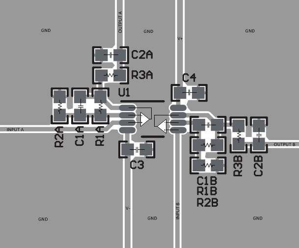
Figure 7-4
Example Layout for TLV9142