SBOSAM4 December 2024 TLV9141 , TLV9144
PRODUCTION DATA
- 1
- 1 Features
- 2 Applications
- 3 Description
- 4 Pin Configuration and Functions
- 5 Specifications
- 6 Detailed Description
- 7 Application and Implementation
- 8 Device and Documentation Support
- 9 Revision History
- 10Mechanical, Packaging, and Orderable Information
パッケージ・オプション
メカニカル・データ(パッケージ|ピン)
サーマルパッド・メカニカル・データ
発注情報
3 Description
The TLV914x family (TLV9141, TLV9142, and TLV9144) is a family of high voltage (18V) rail-to-rail input and output (RRIO) operational amplifiers. These devices offer excellent performance for low-power applications, because of the family's low quiescent current of 7μA/channel.
The TLV914x family offers excellent DC precision, including low offset voltage (±265µV, typical), low offset drift (±0.2µV/°C, typical), short-circuit current limit of 40mA, high PSRR of 140dB, and high CMRR of 108dB for high voltage operation within the main input pair. The devices are also rated to work at wide range of supply voltages from 2.7V to 18V. This makes the TLV914x a flexible, robust, and high-performance op amp for high-voltage industrial applications.
These devices also have a gain bandwidth product of 125kHz and low 1/f flicker noise of 3.4µVpeak-to-peak (0.1Hz to 10Hz). The family was designed to be able to directly drive capacitive loads up to 350nF, while maintaining a phase margin of 30 degrees or higher. The TLV914x op amp family is available in several industry-standard packages and the devices are specified from –40°C to 125°C.
| PART NUMBER | CHANNEL COUNT | PACKAGE(1) | PACKAGE SIZE(2) |
|---|---|---|---|
| TLV9141 | Single | DBV (SOT-23, 5) | 2.9mm × 2.8mm |
| D (SOIC, 8) | 4.9mm × 6mm | ||
| TLV9142 | Dual | PW (TSSOP, 8) | 3mm × 6.4mm |
| D (SOIC, 8) | 4.9mm × 6mm | ||
| TLV9144 | Quad | D (SOIC, 14) | 8.65mm × 6mm |
| PW (TSSOP, 14) | 5mm × 6.4mm | ||
| N (PDIP, 14) | 19.3mm × 7.94mm |
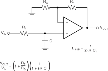
 Single-Pole, Low-Pass Filter