JAJSP86B November 2023 – June 2024 TMAG3001
PRODUCTION DATA
- 1
- 1 特長
- 2 アプリケーション
- 3 概要
- 4 Pin Configuration and Functions
-
5 Specifications
- 5.1 Absolute Maximum Ratings
- 5.2 ESD Ratings
- 5.3 Recommended Operating Conditions
- 5.4 Thermal Information
- 5.5 Electrical Characteristics
- 5.6 Temperature Sensor
- 5.7 Magnetic Characteristics For A1
- 5.8 Magnetic Characteristics For A2
- 5.9 Magnetic Temp Compensation Characteristics
- 5.10 I2C Interface Timing
- 5.11 Power up Timing
- 5.12 Timing Diagram
- 5.13 Typical Characteristics
- 6 Detailed Description
-
7 Application and Implementation
- 7.1
Application Information
- 7.1.1 Select the Sensitivity Option
- 7.1.2 Temperature Compensation for Magnets
- 7.1.3 Sensor Conversion
- 7.1.4 Magnetic Limit Check
- 7.1.5 Magnitude Limit Check
- 7.1.6 Angle Limit Check
- 7.1.7 Switch Mode
- 7.1.8 Error Calculation During Linear Measurement
- 7.1.9 Error Calculation During Angular Measurement
- 7.2 Typical Application
- 7.3 Best Design Practices
- 7.4 Power Supply Recommendations
- 7.5 Layout
- 7.1
Application Information
- 8 Register Map
- 9 Device and Documentation Support
- 10Revision History
- 11Mechanical, Packaging, and Orderable Information
6.5.1 I2C Interface
The TMAG3001 has a standard bidirectional I2C interface that is controlled by a controller device to be configured or read the status of the device. Each target on the I2C bus has a specific device address to differentiate between other target devices that are on the same I2C bus. Many target devices require configuration upon start-up to set the behavior of the device. This is typically done when the controller accesses internal register maps of the target, which have unique register addresses. A device can have one or multiple registers where data is stored, written, or read. At the start bit of an I2C transaction, the conversion result registers are locked to the most recent completed conversion to prevent the results from changing mid transaction. If a conversion is completed mid I2C transaction, the device updates the results register with the new values immediately after the stop condition. The TMAG3001 supports transmission data rates up to 1MHz.
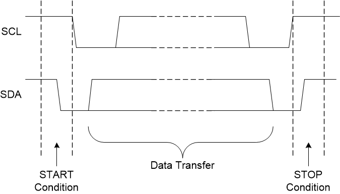
The physical I2C interface consists of the serial clock (SCL) and serial data (SDA) lines. Both SDA and SCL lines must be connected to a supply through a pullup resistor. The size of the pullup resistor is determined by the amount of capacitance on the I2C lines and the communication frequency. For further details, see the I2C Pullup Resistor Calculation application report. Data transfer can only be initiated when the bus is idle. A bus is considered idle if both SDA and SCL lines are high after a STOP condition.
The following is the general procedure for a controller to access a target device:
- If a controller wants to send data to a
target:
- Controller-transmitter sends a START condition and addresses the target-receiver.
- Controller-transmitter sends the requested register to write target-receiver.
- Controller-transmitter sends data to target-receiver.
- Controller-transmitter terminates the transfer with a STOP condition.
- If a controller wants to receive or read
data from a target:
- Controller-receiver sends a START condition and addresses the target-transmitter.
- Controller-receiver sends the requested register to read to target-transmitter.
- Controller-receiver sends a RESTART condition and addresses the target-transmitter.
- Controller-receiver receives data from the target-transmitter.
- Controller-receiver terminates the transfer with a STOP condition.
 Figure 6-11 Definition of Start and Stop Conditions
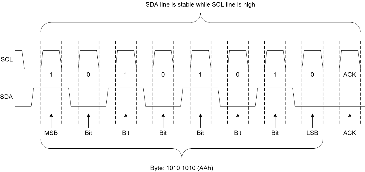
 Figure 6-12 Bit Transfer