JAJSNV0A December   2022  – February 2023 TMAG5115

PRODUCTION DATA  

  1.   1
  2. 特長
  3. アプリケーション
  4. 概要
  5. Revision History
  6. Device Comparison
  7. Pin Configuration and Functions
  8. Specifications
    1. 7.1 Absolute Maximum Ratings
    2. 7.2 ESD Ratings
    3. 7.3 Recommended Operating Conditions
    4. 7.4 Thermal Information
    5. 7.5 Electrical Characteristics
    6. 7.6 Magnetic Characteristics
    7. 7.7 Typical Characteristics
  9. Detailed Description
    1. 8.1 Overview
    2. 8.2 Functional Block Diagram
    3. 8.3 Feature Description
      1. 8.3.1 Field Direction Definition
      2. 8.3.2 Device Output
      3. 8.3.3 Power-On Time
      4. 8.3.4 Output Stage
      5. 8.3.5 Protection Circuits
        1. 8.3.5.1 Short-Circuit Protection
        2. 8.3.5.2 Overtemperature Protection
    4. 8.4 Device Functional Modes
  10. Application and Implementation
    1. 9.1 Application Information
    2. 9.2 Typical Applications
      1. 9.2.1 Standard Circuit
        1. 9.2.1.1 Design Requirements
        2. 9.2.1.2 Detailed Design Procedure
          1. 9.2.1.2.1 Configuration Example
        3. 9.2.1.3 Application Curves
    3. 9.3 Power Supply Recommendations
    4. 9.4 Layout
      1. 9.4.1 Layout Guidelines
      2. 9.4.2 Layout Example
  11. 10Device and Documentation Support
    1. 10.1 Device Support
      1. 10.1.1 Hall Sensor Location
    2. 10.2 ドキュメントの更新通知を受け取る方法
    3. 10.3 サポート・リソース
    4. 10.4 Trademarks
    5. 10.5 静電気放電に関する注意事項
    6. 10.6 用語集
  12. 11Mechanical, Packaging, and Orderable Information

パッケージ・オプション

メカニカル・データ(パッケージ|ピン)
サーマルパッド・メカニカル・データ
発注情報

Output Stage

Figure 8-7 shows the TMAG5115 open-drain NMOS output structure, rated to sink up to 15 mA of current.

Note:

Vref is not restricted to VCC. The allowable voltage range of this pin is specified in the Recommended Operating Conditions.

GUID-958CA50C-08A9-4B8E-B254-1831DA3F1BBD-low.gif Figure 8-7 NMOS Open-Drain Output

Select a value for C2 based on the system bandwidth specifications as shown in Equation 1.

Equation 1. GUID-4F186788-409F-4609-98E5-8031AF38F444-low.gif

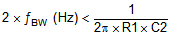
Most applications do not require this C2 filtering capacitor.