JAJSNV0B December 2022 – August 2024 TMAG5115
PRODUCTION DATA
8.2.1.2.1 Configuration Example
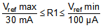
In a 3.3-V system, 3.0V ≤ Vref ≤ 3.6 V. Use Equation 2 to calculate the allowable range for R1.
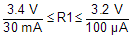
For this design example, use Equation 3 to calculate the allowable range of R1.
Therefore:
After finding the allowable range of R1 (Equation 4), select a value between 500 Ω and 32 kΩ for R1.
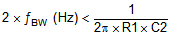
Assuming a system bandwidth of 10 kHz, use Equation 5 to calculate the value of C2.
For this design example, use Equation 6 to calculate the value of C2.
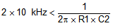
An R1 value of 10 kΩ and a C2 value less than 820 pF satisfy the requirement for a 10-kHz system bandwidth.
A selection of R1 = 10 kΩ and C2 = 680 pF can cause a low-pass filter with a corner frequency of 23.4 kHz.