JAJSJ20A
June 2020 – October 2020
TMAG5124
PRODUCTION DATA
1
1
特長
2
アプリケーション
3
概要
4
Revision History
5
Device Comparison Table
6
Pin Configuration and Functions
7
Specifications
7.1
Absolute Maximum Ratings
7.2
ESD Ratings
7.3
Recommended Operating Conditions
7.4
Thermal Information
7.5
Electrical Characteristics
7.6
Magnetic Characteristics
7.7
Typical Characteristics
7.7.1
TMAG5124A and TMAG5124E
7.7.2
TMAG5124B and TMAG5124F
7.7.3
TMAG5124C and TMAG5124G
7.7.4
TMAG5124D and TMAG5124H
7.7.5
Current Output Level
7.7.5.1
Low-Level Current Output for TMAG5124A/B/C/D
7.7.5.2
Low-Level Current Output for TMAG5124E/F/G/H
7.7.5.3
High-Level Current Output for Every Version
8
Detailed Description
8.1
Overview
8.2
Functional Block Diagram
8.3
Feature Description
8.3.1
Field Direction Definition
8.3.2
Device Output
8.3.3
Protection Circuits
8.3.3.1
Load Dump Protection
8.3.3.2
Reverse Polarity Protection
8.3.4
Power-On Time
8.3.5
Hall Element Location
8.3.6
Propagation Delay
8.3.7
Chopper Stabilization
8.4
Device Functional Modes
9
Application and Implementation
9.1
Application Information
9.2
Typical Applications
9.2.1
High-Side and Low-Side Typical Application Diagrams
9.2.1.1
Design Requirements
9.2.1.2
Detailed Design Procedure
9.2.1.3
Application Curve
10
Power Supply Recommendations
10.1
Power Derating
11
Layout
11.1
Layout Guidelines
11.2
Layout Example
12
Device and Documentation Support
12.1
Documentation Support
12.2
ドキュメントの更新通知を受け取る方法
12.3
サポート・リソース
12.4
Trademarks
12.5
静電気放電に関する注意事項
12.6
用語集
13
Mechanical, Packaging, and Orderable Information
パッケージ・オプション
メカニカル・データ(パッケージ|ピン)
DBZ|3
MPDS108G
サーマルパッド・メカニカル・データ
発注情報
jajsj20a_oa
jajsj20a_pm
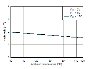
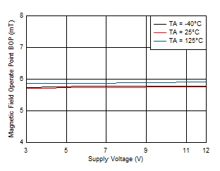
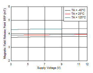
7.7.2
TMAG5124B and TMAG5124F
Figure 7-7
B
OP
vs Temperature
Figure 7-9
B
RP
vs Temperature
Figure 7-11
Hysteresis vs Temperature
Figure 7-8
B
OP
vs V
CC
Figure 7-10
B
RP
vs V
CC
Figure 7-12
Hysteresis vs V
CC