JAJSMQ2 September   2021 TMAG5170

PRODUCTION DATA  

  1. 特長
  2. アプリケーション
  3. 概要
  4. Revision History
  5. Pin Configuration and Functions
  6. Specifications
    1. 6.1 Absolute Maximum Ratings
    2. 6.2 ESD Ratings
    3. 6.3 Recommended Operating Conditions
    4. 6.4 Thermal Information
    5. 6.5 Electrical Characteristics
    6. 6.6 Magnetic Characteristics
    7. 6.7 Power up Timing
    8. 6.8 SPI Interface Timing
    9. 6.9 Typical Characteristics
  7. Detailed Description
    1. 7.1 Overview
    2. 7.2 Functional Block Diagram
    3. 7.3 Feature Description
      1. 7.3.1 Magnetic Flux Direction
      2. 7.3.2 Sensor Location
      3. 7.3.3 Magnetic Range Selection
      4. 7.3.4 Update Rate Settings
      5. 7.3.5 ALERT Function
        1. 7.3.5.1 Interrupt and Trigger Mode
        2. 7.3.5.2 Magnetic Switch Mode
      6. 7.3.6 Threshold Count
      7. 7.3.7 Diagnostics
        1. 7.3.7.1  Memory CRC Check
        2. 7.3.7.2  ALERT Integrity Check
        3. 7.3.7.3  VCC Check
        4. 7.3.7.4  Internal LDO Under Voltage Check
        5. 7.3.7.5  Digital Core Power-on Reset Check
        6. 7.3.7.6  SDO Output Check
        7. 7.3.7.7  Communication CRC Check
        8. 7.3.7.8  Oscillator Integrity Check
        9. 7.3.7.9  Magnetic Field Threshold Check
        10. 7.3.7.10 Temperature Alert Check
        11. 7.3.7.11 Analog Front-End (AFE) Check
        12. 7.3.7.12 Hall Resistance and Switch Matrix Check
        13. 7.3.7.13 Hall Offset Check
        14. 7.3.7.14 ADC Check
    4. 7.4 Device Functional Modes
      1. 7.4.1 Operating Modes
        1. 7.4.1.1 Active Mode
        2. 7.4.1.2 Standby Mode
        3. 7.4.1.3 Configuration Mode (DEFAULT)
        4. 7.4.1.4 Sleep Mode
        5. 7.4.1.5 Wake-Up and Sleep Mode
        6. 7.4.1.6 Deep-Sleep Mode
    5. 7.5 Programming
      1. 7.5.1 Data Definition
        1. 7.5.1.1 Magnetic Sensor Data
        2. 7.5.1.2 Temperature Sensor Data
        3. 7.5.1.3 Magnetic Sensor Offset Correction
        4. 7.5.1.4 Angle and Magnitude Data Definition
      2. 7.5.2 SPI Interface
        1. 7.5.2.1 SCK
        2. 7.5.2.2 CS
        3. 7.5.2.3 SDI
        4. 7.5.2.4 SDO
          1. 7.5.2.4.1 Regular 32-Bit SDO Read
          2. 7.5.2.4.2 Special 32-Bit SDO Read
        5. 7.5.2.5 SPI CRC
        6. 7.5.2.6 SPI Frame
          1. 7.5.2.6.1 32-Bit Read Frame
          2. 7.5.2.6.2 32-Bit Write Frame
    6. 7.6 Register Map
      1. 7.6.1 TMAG5170 Registers
  8. Application and Implementation
    1. 8.1 Application Information
      1. 8.1.1 Selecting the Sensitivity Option
      2. 8.1.2 Temperature Compensation for Magnets
      3. 8.1.3 Sensor Conversion
        1. 8.1.3.1 Continuous Conversion
        2. 8.1.3.2 Trigger Conversion
        3. 8.1.3.3 Pseudo-Simultaneous Sampling
      4. 8.1.4 Error Calculation During Linear Measurement
      5. 8.1.5 Error Calculation During Angular Measurement
    2. 8.2 Typical Application
      1. 8.2.1 Design Requirements
        1. 8.2.1.1 Gain Adjustment for Angle Measurement
      2. 8.2.2 Detailed Design Procedure
      3. 8.2.3 Application Curves
    3. 8.3 Do's and Don'ts
  9. Power Supply Recommendations
  10. 10Layout
    1. 10.1 Layout Guidelines
    2. 10.2 Layout Example
  11. 11Device and Documentation Support
    1. 11.1 Receiving Notification of Documentation Updates
    2. 11.2 サポート・リソース
    3. 11.3 Trademarks
    4. 11.4 Electrostatic Discharge Caution
    5. 11.5 Glossary
  12. 12Mechanical, Packaging, and Orderable Information

パッケージ・オプション

メカニカル・データ(パッケージ|ピン)
サーマルパッド・メカニカル・データ
発注情報

Magnetic Sensor Data

The X, Y, and Z magnetic sensor data are stored in the X_CH_RESULT, Y_CH_RESULT, and Z_CH_RESULT registers, respectively. The 12-bit ADC output is stored in 16-bit result registers in 2's complement format as shown in Figure 7-5. With fastest conversion (CONV_AVG = 000b), the ADC output loads the 12 MSB bits of the 16-bit result register along with 4 LSB bits as zeros. With CONV_AVG ≠ 000b, all the 16 bits are used to store the results. With DATA_TYPE = 00b, the 16-bit magnetic sensor data can be accessed through regular 32-bit SPI read. Use Equation 5 to calculate the measured magnetic field.

Equation 1. B = - ( D 15 × 2 15 ) + i = 0 14 D i × 2 i 2 16 × 2 B R

where

  • B is magnetic field in mT.
  • Di is the data bit as shown in Figure 7-5.
  • BR is the magnetic range in mT for the corresponding channel.
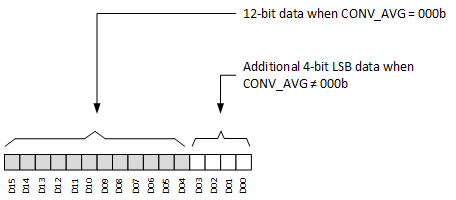
GUID-C0B91973-180B-46F5-9794-892BBA7A3B67-low.gif Figure 7-5 Magnetic Sensor Data Definition

With DATA_TYPE ≠ 00b, the 12 MSB bits (D04 to D15) from the magnetic result registers can be accessed. In this mode, use Equation 2 to calculate the measured magnetic field.

Equation 2. B = - ( D 15 × 2 11 ) + i = 4 14 D i × 2 i - 4 2 12 × 2 B R