SBOS685C April 2014 – July 2015 TMP007
PRODUCTION DATA.
- 1 Features
- 2 Applications
- 3 Description
- 4 Revision History
- 5 Pin Configuration and Functions
- 6 Specifications
-
7 Detailed Description
- 7.1 Overview
- 7.2 Functional Block Diagram
- 7.3
Feature Description
- 7.3.1 Spectral Responsivity
- 7.3.2 Field of View and Angular Response
- 7.3.3 Thermopile Principles and Operation
- 7.3.4 Object Temperature Calculation
- 7.3.5 Calibration
- 7.3.6 Sensor Voltage Format
- 7.3.7 Temperature Format
- 7.3.8 Serial Interface
- 7.4 Device Functional Modes
- 7.5
Register Maps
- 7.5.1 Sensor Voltage Result Register (address = 00h) [reset = 0000h]
- 7.5.2 TDIE Local Temperature Result Register (address = 01h) [reset = 0000h]
- 7.5.3 Configuration Register (address = 02h) [reset = 1440h]
- 7.5.4 TOBJ Object Temperature Result Register (address = 03h) [reset = 0000h]
- 7.5.5 Status Register (address = 04h) [reset = 0000h]
- 7.5.6 Status Mask and Enable Register (address = 05h) [reset = 0000h]
- 7.5.7 TOBJ Object Temperature High-Limit Register (address = 06h) [reset = 7FC0h]
- 7.5.8 TOBJ Object Temperature Low-Limit Register (address = 07h) [reset = 8000h]
- 7.5.9 TDIE Local Temperature High-Limit Register (address = 08h) [reset = 7FC0h]
- 7.5.10 TDIE Local Temperature Low-Limit Register (address = 09h) [reset = 8000h]
- 7.5.11
Coefficient Registers
- 7.5.11.1 S0 Coefficient Register (address = 0Ah) [reset = 260Eh]
- 7.5.11.2 A1 Coefficient Register (address = 0Bh) [reset = 0106h]
- 7.5.11.3 A2 Coefficient Register (address = 0Ch) [reset = FF9Bh]
- 7.5.11.4 B0 Coefficient Register (address = 0Dh) [reset = FF3Ah]
- 7.5.11.5 B1 Coefficient Register (address = 0Eh) [reset = FF71h]
- 7.5.11.6 B2 Coefficient Register (address = 0Fh) [reset = 0553h]
- 7.5.11.7 C2 Coefficient Register (address = 10h) [reset = 0000h]
- 7.5.11.8 TC0 Coefficient Register (address = 11h) [reset = 0034h]
- 7.5.11.9 TC1 Coefficient Register (address = 12h) [reset = 0000h]
- 7.5.12 Manufacturer ID Register (address = 1Eh) [reset = 5449h]
- 7.5.13 Device ID Register (address = 1Fh) [reset = 0078h]
- 7.5.14 Memory Access Register (address = 2Ah) [reset = 0000h]
- 8 Application and Implementation
- 9 Power-Supply Recommendations
- 10Layout
- 11Device and Documentation Support
- 12Mechanical, Packaging, and Orderable Information
6 Specifications
6.1 Absolute Maximum Ratings
over operating free-air temperature range (unless otherwise noted) (1)(2)(1) Stresses beyond those listed under Absolute Maximum Ratings may cause permanent damage to the device. These are stress ratings only, which do not imply functional operation of the device at these or any other conditions beyond those indicated under Recommended Operating Conditions. Exposure to absolute-maximum-rated conditions for extended periods may affect device reliability.
(2) Input voltage rating applies to all TMP007 input voltages.
6.2 ESD Ratings
| VALUE | UNIT | |||
|---|---|---|---|---|
| V(ESD) | Electrostatic discharge | Human-body model (HBM), per ANSI/ESDA/JEDEC JS-001(1) | ±2000 | V |
| Charged-device model (CDM), per JEDEC specification JESD22-C101(2) | ±500 | |||
| Machine model | ±200 | |||
(1) JEDEC document JEP155 states that 500-V HBM allows safe manufacturing with a standard ESD control process.
(2) JEDEC document JEP157 states that 250-V CDM allows safe manufacturing with a standard ESD control process.
6.3 Recommended Operating Conditions
over operating free-air temperature range (unless otherwise noted)| MIN | NOM | MAX | UNIT | ||
|---|---|---|---|---|---|
| Supply voltage, VS | 2.5 | 3.3 | 5.5 | V | |
| Operating temperature range | –40 | +125 | °C | ||
| Die temperature, TDIE | 125 | °C | |||
| Object temperature, TOBJ | See note (1) | °C | |||
(1) Object temperature is application dependent.
6.4 Thermal Information
| THERMAL METRIC(1) | TMP007 | UNIT | |
|---|---|---|---|
| YZF (DSBGA) | |||
| 8 PINS | |||
| RθJA | Junction-to-ambient thermal resistance | 115.3 | °C/W |
| RθJC(top) | Junction-to-case (top) thermal resistance | 0.4 | °C/W |
| RθJB | Junction-to-board thermal resistance | 14.3 | °C/W |
| ψJT | Junction-to-top characterization parameter | 3.8 | °C/W |
| ψJB | Junction-to-board characterization parameter | 14.1 | °C/W |
| RθJC(bot) | Junction-to-case (bottom) thermal resistance | N/A | °C/W |
(1) For more information about traditional and new thermal metrics, see the IC Package Thermal Metrics application report, SPRA953.
6.5 Electrical Characteristics
at TDIE = 25°C, and V+ = +3.3 V (unless otherwise noted)| PARAMETER | TEST CONDITIONS | MIN | TYP | MAX | UNIT | |
|---|---|---|---|---|---|---|
| DEVICE PERFORMANCE | ||||||
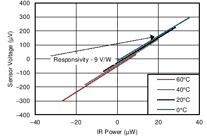
| Responsivity (signal) | TDIE = 0°C to 100°C, TOBJ = 0°C to 60°C | 9 | V/W | |||
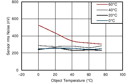
| Sensor noise | 1-s conversion, TDIE = 0°C to 60°C, TOBJ = 0°C to 60°C | 300 | nVrms | |||
| Noise equivalent power (NEP) | At 1 σ, TDIE = 0°C to 60°C, TOBJ = 0°C to 60°C | 32 | nW | |||
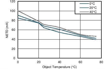
| Noise equivalent temperature difference(1)(NETD) | TDIE = 0°C to 60°C, TOBJ = 0°C to 60°C | 90 | mK | |||
| Noise equivalent temperature difference (NETD) | At F/1 (6 σ), TDIE = 25°C, TOBJ = 0°C to 60°C | 1.4 | °C | |||
| Absorber size | 330 × 330 | μm | ||||
| REFERENCE SYSTEM PERFORMANCE(1) | ||||||
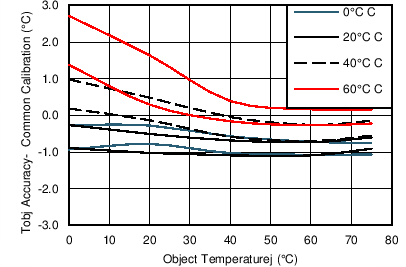
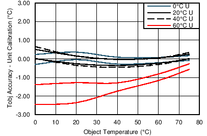
| Object temperature accuracy(1) (error) | TDIE = 20°C to 40°C, TOBJ = 20°C to 60°C | ±1 | ±3 | °C | ||
| TDIE = 0°C to 60°C, TOBJ = –15°C to 85°C | ±2 | ±5 | °C | |||
| TEMPERATURE MEASUREMENT | ||||||
| TDIE | Die temperature range | –40 | +125 | °C | ||
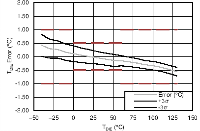
| TDIE accuracy (error) | ±0.5 | ±1 | °C | |||
| Accuracy vs supply | ±0.1 | ±0.2 | °C/V | |||
| Conversion time | 0.25 | Second | ||||
| Temperature resolution (object and local) | 0.03125 | °C/LSB | ||||
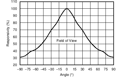
| Field of view (50% responsivity, full angle) | 90 | Degrees | ||||
| DIGITAL PINS | ||||||
| VIH | High-level input voltage | 1.4 | V | |||
| VIL | Low-level input voltage | 0.4 | V | |||
| Hysteresis | 200 | mV | ||||
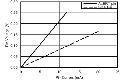
| VOL | Low-level output voltage, SDA | IOUT = –6 mA | 0.05 | 0.4 | V | |
| Output ALERT logic low sink | IOUT = –6 mA | 0.200 | V | |||
| IIN | Input current | 0 V < VIN < 5.5 V | –1 | +1 | µA | |
| Input capacitance | 3 | pF | ||||
| SMBus frequency | 0.01 | 2.5 | MHz | |||
| Timeout time | 25 | 28 | 35 | ms | ||
| POWER SUPPLY | ||||||
| V+ | Operating supply range | 2.5 | 5.5 | V | ||
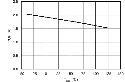
| POR | Power-on reset | 1.9 | V | |||
| Nonvolatile memory programming voltage | 2.5 | 5.5 | V | |||
| Nonvolatile memory programming current | Supply current pulse time < 3 ms | 2.8 | mA | |||
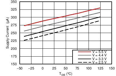
| IQ | Quiescent current | Serial bus inactive, continuous conversion | 270 | 350 | µA | |
| Low power conversion, serial bus inactive, CR2 = 1, CR1 = x, CR0 = 1 | 85(2) | µA | ||||
| Low power conversion serial bus active, CR2 = 1, CR1 = 1, CR0 = 0 | 60(2) | µA | ||||
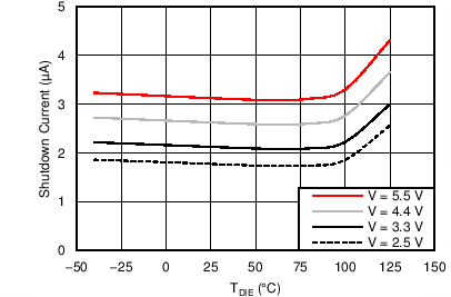
| ISD | Shutdown current | Serial bus inactive | 2 | 4 | µA | |
| Serial bus active, 400 kHz | 36 | µA | ||||
(1) This parameter is tested in a fully-settled setup with no transients, in front of a black body, ε = 0.95, field of view (FOV) = 110°, with the recommended layout , and after system calibration with a common set of coefficients loaded.
(2) Average current over complete measurement cycle.
6.6 Typical Characteristics
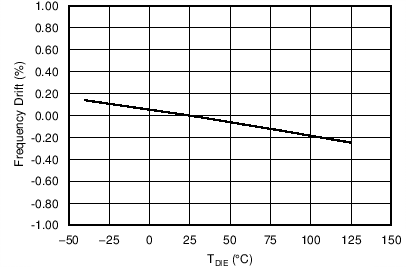
at TDIE = 25°C, and V+ = +3.3 V (unless otherwise noted)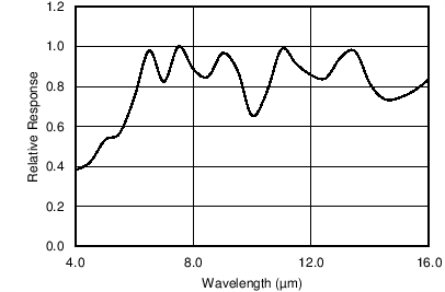
INDENT:
NOTE: The responsivity is the slope of the lines.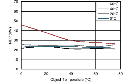
NOTE:
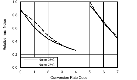
NOTE: In the last three conversion modes, there is a change in sensor voltage, and a different set of calibration coefficients may be needed depending on the accuracy required.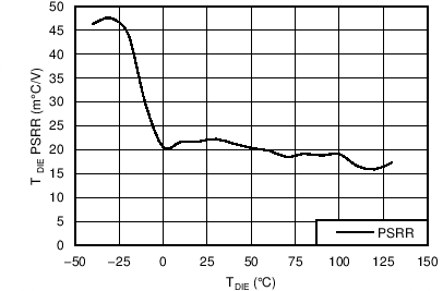
| 2.5 V < VS < 5.5 V | ||
