JAJS306I August   2007  – June 2024 TMP102

PRODUCTION DATA  

  1.   1
  2. 特長
  3. アプリケーション
  4. 概要
  5. Pin Configuration and Functions
  6. Specifications
    1. 5.1 Absolute Maximum Ratings
    2. 5.2 ESD Ratings
    3. 5.3 Recommended Operating Conditions
    4. 5.4 Thermal Information
    5. 5.5 Electrical Characteristics
    6. 5.6 Timing Requirements
    7. 5.7 Typical Characteristics
  7. Detailed Description
    1. 6.1 Overview
    2. 6.2 Functional Block Diagram
    3. 6.3 Feature Description
      1. 6.3.1  Digital Temperature Output
      2. 6.3.2  Serial Interface
      3. 6.3.3  Bus Overview
      4. 6.3.4  Serial Bus Address
      5. 6.3.5  Writing and Reading Operation
      6. 6.3.6  Target Mode Operations
        1. 6.3.6.1 Target Receiver Mode
        2. 6.3.6.2 Target Transmitter Mode
      7. 6.3.7  SMBus Alert Function
      8. 6.3.8  General Call
      9. 6.3.9  High-Speed (HS) Mode
      10. 6.3.10 Timeout Function
      11. 6.3.11 Timing Diagrams
    4. 6.4 Device Functional Modes
      1. 6.4.1 Continuous-Conversion Mode
      2. 6.4.2 Extended Mode (EM)
      3. 6.4.3 Shutdown Mode (SD)
      4. 6.4.4 One-Shot/Conversion Ready (OS)
      5. 6.4.5 Thermostat Mode (TM)
        1. 6.4.5.1 Comparator Mode (TM = 0)
        2. 6.4.5.2 Interrupt Mode (TM = 1)
    5. 6.5 Programming
      1. 6.5.1 Pointer Register
      2. 6.5.2 Temperature Register
      3. 6.5.3 Configuration Register
        1. 6.5.3.1 Shutdown Mode (SD)
        2. 6.5.3.2 Thermostat Mode (TM)
        3. 6.5.3.3 Polarity (POL)
        4. 6.5.3.4 Fault Queue (F1/F0)
        5. 6.5.3.5 Converter Resolution (R1/R0)
        6. 6.5.3.6 One-Shot (OS)
        7. 6.5.3.7 EM Bit
        8. 6.5.3.8 Alert (AL Bit)
        9. 6.5.3.9 Conversion Rate (CR)
      4. 6.5.4 High- and Low-Limit Registers
  8. Application and Implementation
    1. 7.1 Application Information
    2. 7.2 Typical Application
      1. 7.2.1 Design Requirements
      2. 7.2.2 Detailed Design Procedure
      3. 7.2.3 Application Curve
    3. 7.3 Power Supply Recommendations
    4. 7.4 Layout
      1. 7.4.1 Layout Guidelines
      2. 7.4.2 Layout Example
  9. Device and Documentation Support
    1. 8.1 Documentation Support
      1. 8.1.1 Related Documentation
    2. 8.2 ドキュメントの更新通知を受け取る方法
    3. 8.3 サポート・リソース
    4. 8.4 Trademarks
    5. 8.5 静電気放電に関する注意事項
    6. 8.6 用語集
  10. Revision History
  11. 10Mechanical, Packaging, and Orderable Information

パッケージ・オプション

メカニカル・データ(パッケージ|ピン)
サーマルパッド・メカニカル・データ
発注情報

Detailed Design Procedure

Place the TMP102 device in close proximity to the heat source that must be monitored, with a proper layout for good thermal coupling. This placement verifies that temperature changes are captured within the shortest possible time interval. To maintain accuracy in applications that require air or surface temperature measurement, care must be taken to isolate the package and leads from ambient air temperature. A thermally-conductive adhesive is helpful in achieving accurate surface temperature measurement.

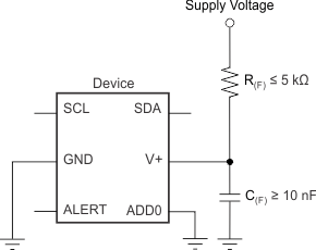
The TMP102 device is a very low-power device and generates very low noise on the supply bus. Applying an RC filter to the V+ pin of the TMP102 device can further reduce any noise that the TMP102 device can propagate to other components. R(F) in Figure 7-2 must be less than 5 kΩ and C(F) must be greater than 10 nF.
TMP102 Noise Reduction TechniquesFigure 7-2 Noise Reduction Techniques