JAJSLQ4C May 2021 – June 2022 TMP126-Q1
PRODUCTION DATA
- 1 特長
- 2 アプリケーション
- 3 概要
- 4 Revision History
- 5 Device Comparison
- 6 Pin Configuration and Functions
- 7 仕様
-
8 Detailed Description
- 8.1 Overview
- 8.2 Functional Block Diagram
- 8.3 Feature Descriptions
- 8.4 Device Functional Modes
- 8.5 Programming
- 8.6 Register Map
- 9 Application and Implementation
- 10Power Supply Recommendations
- 11Layout
- 12Device and Documentation Support
- 13Mechanical, Packaging, and Orderable Information
パッケージ・オプション
メカニカル・データ(パッケージ|ピン)
サーマルパッド・メカニカル・データ
発注情報
8.4.4.1 Interrupt Mode
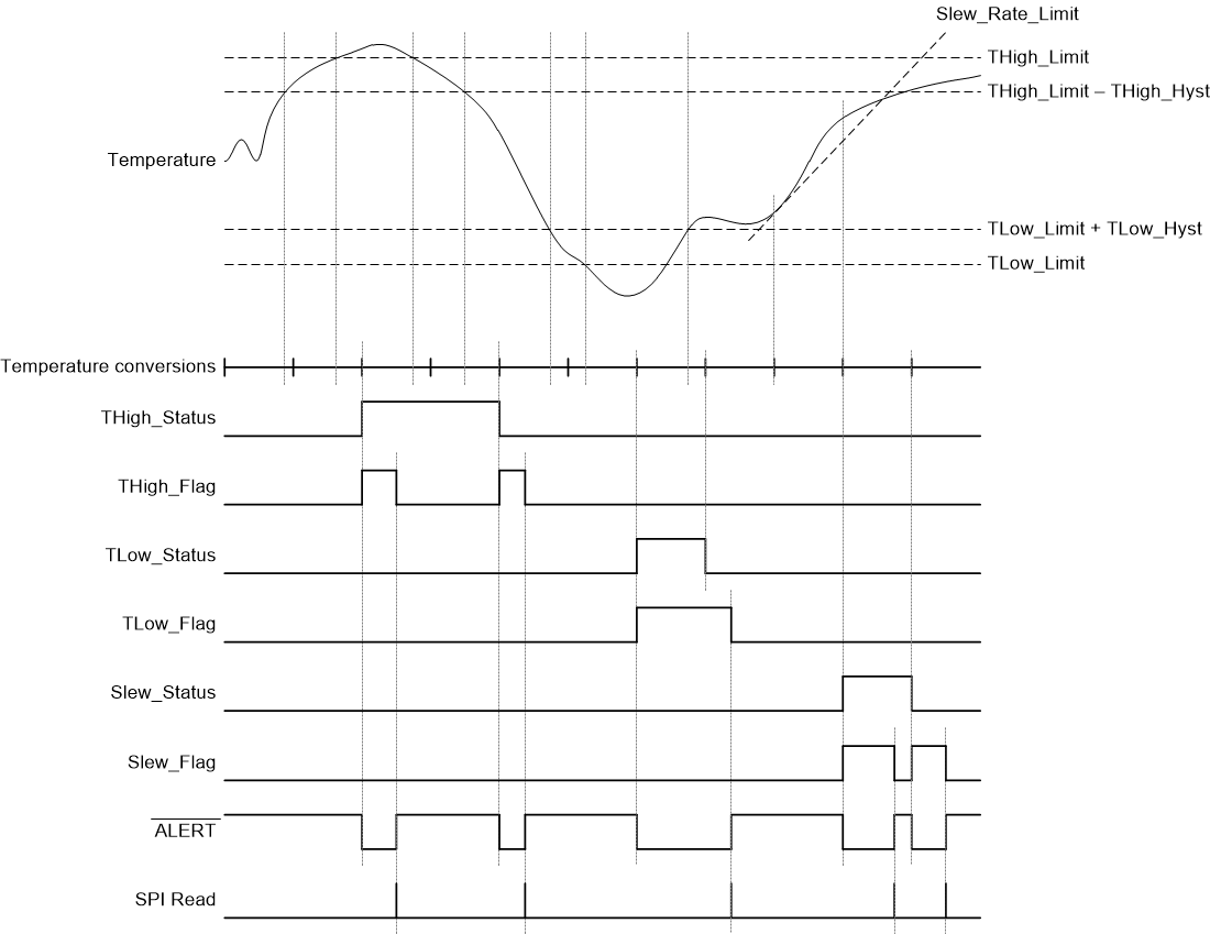
When the INT_COMP bit in the Configuration register is set to 0, the device is in interrupt mode. Changing the device to Interrupt mode from Comparator mode will immediately clear the Alert_Status register and reset the ALERT pin. The TMP126-Q1 will then behave as described in this section at the next temperature conversion. In this mode, the device compares the temperature result at the end of every conversion with the values in the TLow_Limit register and THigh_Limit register. If the temperature result is higher the value in the THigh_Limit register, the THigh_Status and THigh_Flag bits in the Alert_Status register will be set and the ALERT pin will assert. After a read of the Alert_Status register the flag bit will clear and the ALERT pin will de-assert. Subsequent temperature results above the hysteresis value (THigh_Limit - THigh_Hysteresis), where THigh_Hysteresis is the Most Significant Byte (MSB) in the Hysteresis register, will not set the THigh_Flag bit. The status bit will not clear until a temperature result is below (THigh_Limit - THigh_Hysteresis).
After a temperature result below (THigh_Limit - THigh_Hysteresis), the THigh_Status bit will clear, the THigh_Flag bit will be set, and the ALERT pin will be asserted to indicate the change.
If the THigh_Flag bit is not enabled in the Alert_Enable register, the flag bit will be set when the measured temperature crosses the THigh_Limit or hysteresis but the ALERT pin will not assert. The behavior for the TLow_Limit and Slew rate will be the same as the previously described high limit. Figure 8-7 shows a diagram depicting the behavior.
 Figure 8-7 Interrupt Mode Diagram