SLDS153B May 2009 – November 2015 TMP815
PRODUCTION DATA.
8 Application and Implementation
NOTE
Information in the following applications sections is not part of the TI component specification, and TI does not warrant its accuracy or completeness. TI’s customers are responsible for determining suitability of components for their purposes. Customers should validate and test their design implementation to confirm system functionality.
8.1 Application Information
The TMP815 device needs few external components for the features described in Feature Description . The device needs a 1-uF or greater capacitor connected at VCC. The device generates 5-V regulated output which can be used for pullups in the circuit as well as the Hall sensor.
8.2 Typical Application
Figure 5 shows the typical application diagram.
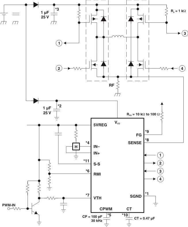 Figure 5. 12-V Sample Application Circuit
8.2.1 Design Requirements
For this design example, use the following parameters:
- Input Voltage: 6 to 16 V
- VCC capacitor: 1 µF or more
- H Bridge top side: P-channel FETs
- H Bridge bottom side: N-channel FETs
8.2.2 Detailed Design Procedure
Pins:
- CPWM Capacitor: 220 pF for 30-kHz switching or appropriate.
- VTH Pin connected to Ground for Full speed or supplied with pulsed input
- RMI Pin Pulled high to 5VREG output or external connection if required
- 5VREG connected to Hall Sensor. Hall sensor differential inputs connected to IN+ and IN-
- Current sense resistor connected to SENSE pin or GND.
- CT connected to Lock Detection capacitor (0.47 uF or calculated values) or to GND
- Drive outputs connected to the Gates of the H bridge switches.
- Pull up on FG.
Power Supply:
- Make sure the power supply has set with sufficient current limit at the decided at the motor voltage.
Build the circuit with the recommended connections at the pins.
Test the motor circuit with hardware connected to it.
8.2.3 Application Curves
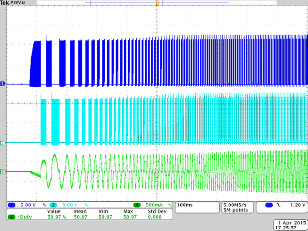 Figure 6. Start-up at 12 V (Soft Start)
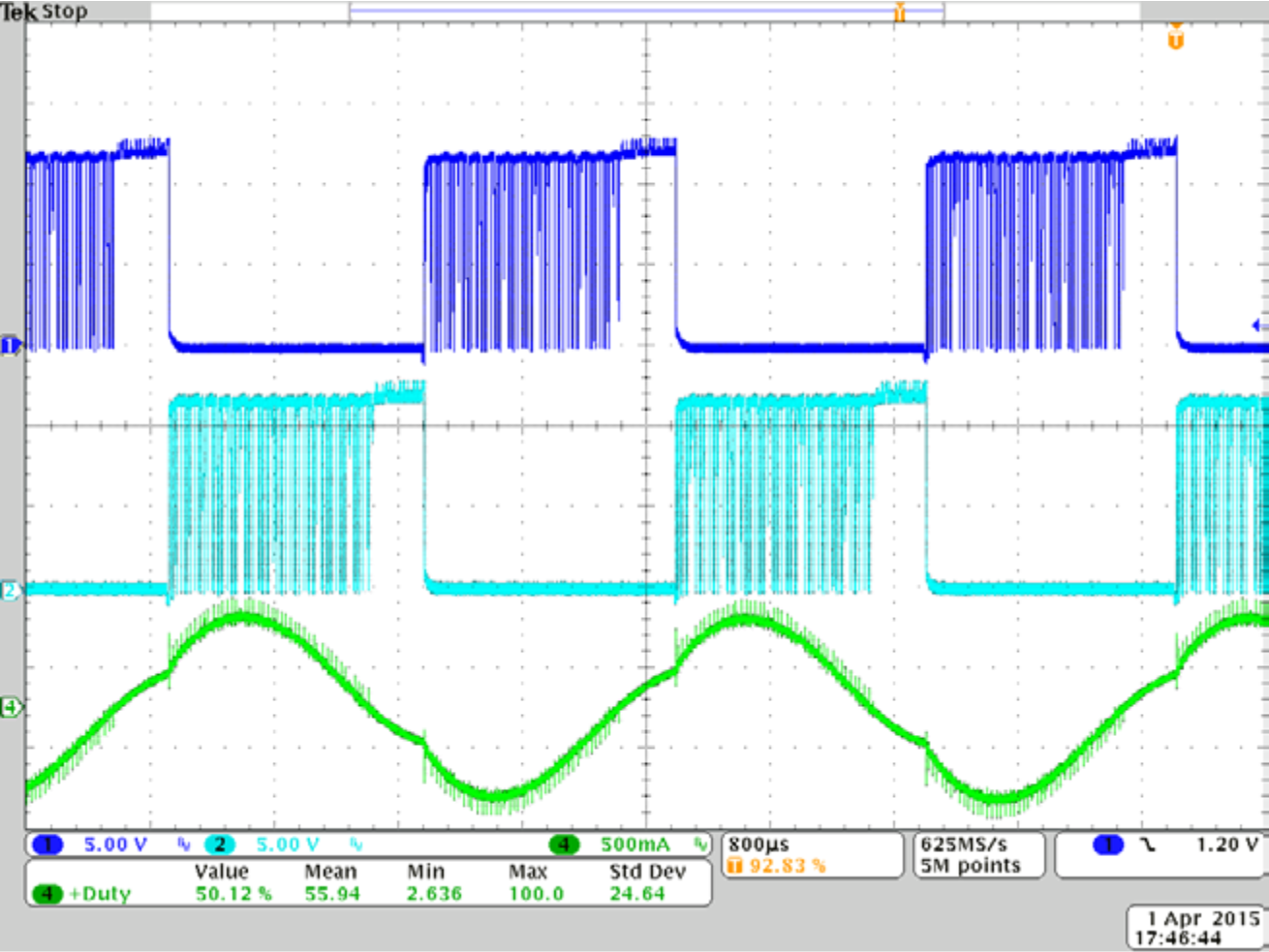 Figure 8. Motor Outputs and Phase Current at Duty Cycle < 100%
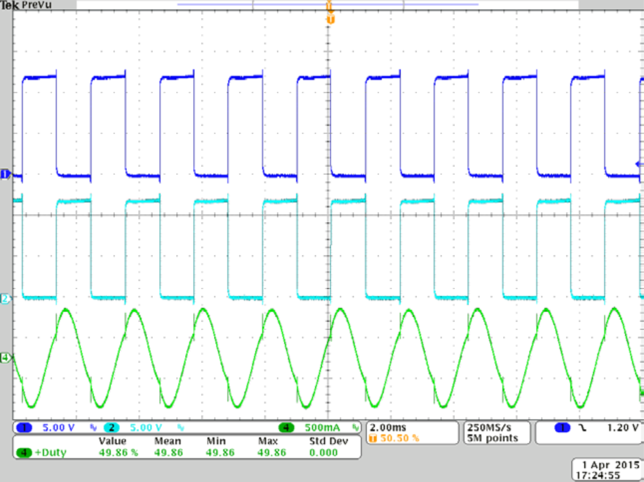 Figure 7. Motor Outputs and Phase Current at 100% Duty Cycle
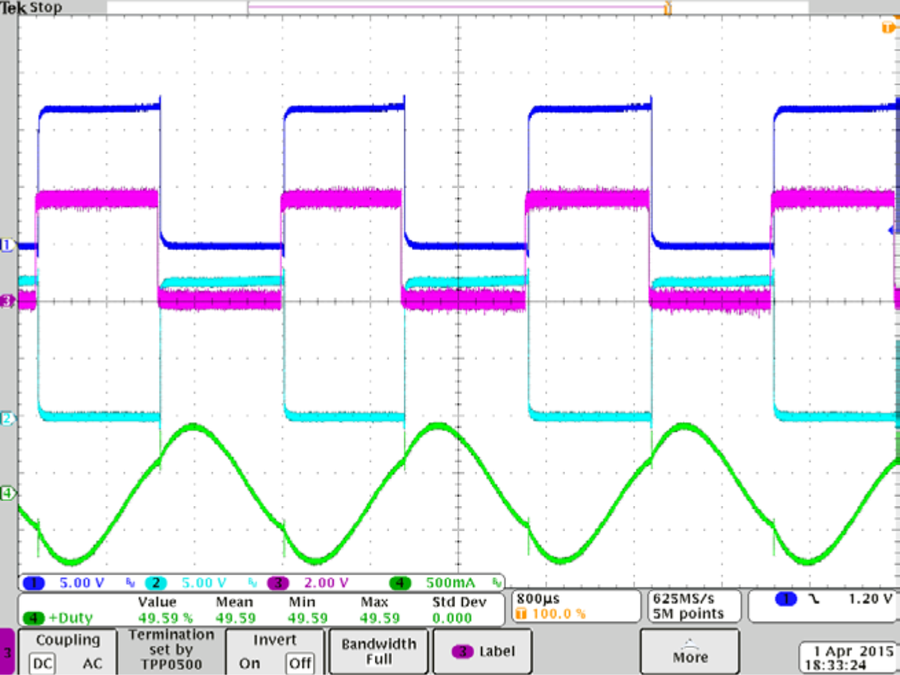 Figure 9. Motor Outputs and Phase Currents at 100% Duty Cycle and With Hall Sensor Data