JAJSFZ4E March 2009 – August 2018 TMS320C28341 , TMS320C28342 , TMS320C28343 , TMS320C28344 , TMS320C28345 , TMS320C28346
PRODUCTION DATA.
- 1デバイスの概要
- 2改訂履歴
- 3Device Comparison
- 4Terminal Configuration and Functions
-
5Specifications
- 5.1 Absolute Maximum Ratings
- 5.2 ESD Ratings – Automotive
- 5.3 ESD Ratings – Commercial
- 5.4 Recommended Operating Conditions
- 5.5 Power Consumption Summary
- 5.6 Electrical Characteristics
- 5.7 Thermal Resistance Characteristics
- 5.8 Thermal Design Considerations
- 5.9
Timing and Switching Characteristics
- 5.9.1 Timing Parameter Symbology
- 5.9.2 Power Sequencing
- 5.9.3 Clock Requirements and Characteristics
- 5.9.4
Peripherals
- 5.9.4.1 General-Purpose Input/Output (GPIO)
- 5.9.4.2 Enhanced Control Peripherals
- 5.9.4.3 External Interrupt Timing
- 5.9.4.4 I2C Electrical Specification and Timing
- 5.9.4.5 Serial Peripheral Interface (SPI) Timing
- 5.9.4.6
Multichannel Buffered Serial Port (McBSP) Timing
- 5.9.4.6.1 McBSP Transmit and Receive Timing
- 5.9.4.6.2
McBSP as SPI Master or Slave Timing
- Table 5-36 McBSP as SPI Master or Slave Timing Requirements (CLKSTP = 10b, CLKXP = 0)
- Table 5-37 McBSP as SPI Master or Slave Switching Characteristics (CLKSTP = 10b, CLKXP = 0)
- Table 5-38 McBSP as SPI Master or Slave Timing Requirements (CLKSTP = 11b, CLKXP = 0)
- Table 5-39 McBSP as SPI Master or Slave Switching Characteristics (CLKSTP = 11b, CLKXP = 0)
- Table 5-40 McBSP as SPI Master or Slave Timing Requirements (CLKSTP = 10b, CLKXP = 1)
- Table 5-41 McBSP as SPI Master or Slave Switching Characteristics (CLKSTP = 10b, CLKXP = 1)
- Table 5-42 McBSP as SPI Master or Slave Timing Requirements (CLKSTP = 11b, CLKXP = 1)
- Table 5-43 McBSP as SPI Master or Slave Switching Characteristics (CLKSTP = 11b, CLKXP = 1)
- 5.9.5 Emulator Connection Without Signal Buffering for the MCU
- 5.9.6
External Interface (XINTF) Timing
- 5.9.6.1 USEREADY = 0
- 5.9.6.2 Synchronous Mode (USEREADY = 1, READYMODE = 0)
- 5.9.6.3 Asynchronous Mode (USEREADY = 1, READYMODE = 1)
- 5.9.6.4 XINTF Signal Alignment to XCLKOUT
- 5.9.6.5 External Interface Read Timing
- 5.9.6.6 External Interface Write Timing
- 5.9.6.7
External Interface Ready-on-Read Timing With One External Wait State
- Table 5-49 External Interface Read Switching Characteristics (Ready-on-Read, One Wait State)
- Table 5-50 External Interface Read Timing Requirements (Ready-on-Read, One Wait State)
- Table 5-51 Synchronous XREADY Timing Requirements (Ready-on-Read, One Wait State)
- Table 5-52 Asynchronous XREADY Timing Requirements (Ready-on-Read, One Wait State)
- 5.9.6.8 External Interface Ready-on-Write Timing With One External Wait State
- 5.9.6.9 XHOLD and XHOLDA Timing
-
6Detailed Description
- 6.1
Brief Descriptions
- 6.1.1 C28x CPU
- 6.1.2 Memory Bus (Harvard Bus Architecture)
- 6.1.3 Peripheral Bus
- 6.1.4 Real-Time JTAG and Analysis
- 6.1.5 External Interface (XINTF)
- 6.1.6 M0, M1 SARAMs
- 6.1.7 L0, L1, L2, L3, L4, L5, L6, L7, H0, H1, H2, H3, H4, H5 SARAMs
- 6.1.8 Boot ROM
- 6.1.9 Security
- 6.1.10 Peripheral Interrupt Expansion (PIE) Block
- 6.1.11 External Interrupts (XINT1–XINT7, XNMI)
- 6.1.12 Oscillator and PLL
- 6.1.13 Watchdog
- 6.1.14 Peripheral Clocking
- 6.1.15 Low-Power Modes
- 6.1.16 Peripheral Frames 0, 1, 2, 3 (PFn)
- 6.1.17 General-Purpose Input/Output (GPIO) Multiplexer
- 6.1.18 32-Bit CPU-Timers (0, 1, 2)
- 6.1.19 Control Peripherals
- 6.1.20 Serial Port Peripherals
- 6.2
Peripherals
- 6.2.1 DMA Overview
- 6.2.2 32-Bit CPU-Timer 0, CPU-Timer 1, CPU-Timer 2
- 6.2.3 Enhanced PWM Modules
- 6.2.4 High-Resolution PWM (HRPWM)
- 6.2.5 Enhanced CAP Modules
- 6.2.6 Enhanced QEP Modules
- 6.2.7 External ADC Interface
- 6.2.8 Multichannel Buffered Serial Port (McBSP) Module
- 6.2.9 Enhanced Controller Area Network (eCAN) Modules (eCAN-A and eCAN-B)
- 6.2.10 Serial Communications Interface (SCI) Modules (SCI-A, SCI-B, SCI-C)
- 6.2.11 Serial Peripheral Interface (SPI) Module (SPI-A, SPI-D)
- 6.2.12 Inter-Integrated Circuit (I2C)
- 6.2.13 GPIO MUX
- 6.2.14 External Interface (XINTF)
- 6.3 Memory Maps
- 6.4 Register Map
- 6.5 Interrupts
- 6.6 System Control
- 6.7 Low-Power Modes Block
- 6.1
Brief Descriptions
- 7Applications, Implementation, and Layout
- 8デバイスおよびドキュメントのサポート
- 9メカニカル、パッケージ、および注文情報
パッケージ・オプション
デバイスごとのパッケージ図は、PDF版データシートをご参照ください。
メカニカル・データ(パッケージ|ピン)
- ZFE|256
サーマルパッド・メカニカル・データ
発注情報
Table 5-52 Asynchronous XREADY Timing Requirements (Ready-on-Read, One Wait State)
| MIN | MAX | UNIT | ||
|---|---|---|---|---|
| tsu(XRDYAsynchL)XCOHL | Setup time, XREADY (asynchronous) low before XCLKOUT high/low | 8 | ns | |
| th(XRDYAsynchL) | Hold time, XREADY (asynchronous) low | 1tc(XTIM) | ns | |
| tsu(XRDYAsynchH)XCOHL | Setup time, XREADY (asynchronous) high before XCLKOUT high/low | 8 | ns | |
| th(XRDYasynchH)XZCSH | Hold time, XREADY (asynchronous) held high after zone chip select high | 0 | ns | |

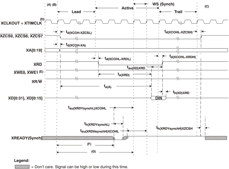
A. All XINTF accesses (lead period) begin on the rising edge of XCLKOUT. When necessary, the device inserts an alignment cycle before an access to meet this requirement.
B. During alignment cycles, all signals transition to their inactive state.
C. During inactive cycles, the XINTF address bus always holds the last address put out on the bus except XA0, which remains high. This includes alignment cycles.
D. Timings are also relevant for XCLKOUT = 1/2 XTIMCLK and XCLKOUT = 1/4 XTIMCLK.
E. XWE1 is valid only in 32-bit data bus mode.
F. For each sample, setup time from the beginning of the access (E) can be calculated as:
D = (XRDLEAD + XRDACTIVE +n - 1) tc(XTIM) – tsu(XRDYsynchL)XCOHL
D = (XRDLEAD + XRDACTIVE +n - 1) tc(XTIM) – tsu(XRDYsynchL)XCOHL
G. Reference for the first sample is with respect to this point: F = (XRDLEAD + XRDACTIVE) tc(XTIM) where n is the sample number: n = 1, 2, 3, and so forth.
Figure 5-30 Example Read With Synchronous XREADY Access XTIMING register parameters used for this example (based on 300-MHz system clock):
| XRDLEAD | XRDACTIVE | XRDTRAIL | USEREADY | X2TIMING | XWRLEAD | XWRACTIVE | XWRTRAIL | READYMODE |
|---|---|---|---|---|---|---|---|---|
| ≥ 2 | 5 | ≥ 0 | 1 | 0 | N/A(1) | N/A(1) | N/A(1) | 0 = XREADY (Synch) |
(1) N/A = “Don’t care” for this example

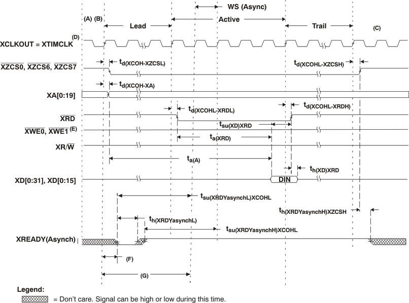
A. All XINTF accesses (lead period) begin on the rising edge of XCLKOUT. When necessary, the device will insert an alignment cycle before an access to meet this requirement.
B. During alignment cycles, all signals will transition to their inactive state.
C. During inactive cycles, the XINTF address bus will always hold the last address put out on the bus except XA0, which remains high. This includes alignment cycles.
D. Timings are also relevant for XCLKOUT = 1/2 XTIMCLK and XCLKOUT = 1/4 XTIMCLK.
E. XWE1 is valid only in 32-bit data bus mode.
F. For each sample, setup time from the beginning of the access can be calculated as:
E = (XRDLEAD + XRDACTIVE -3 +n) tc(XTIM) – tsu(XRDYasynchL)XCOHL where n is the sample number: n = 1, 2, 3, and so forth.
E = (XRDLEAD + XRDACTIVE -3 +n) tc(XTIM) – tsu(XRDYasynchL)XCOHL where n is the sample number: n = 1, 2, 3, and so forth.
G. Reference for the first sample is with respect to this point: F = (XRDLEAD + XRDACTIVE –2) tc(XTIM)
Figure 5-31 Example Read With Asynchronous XREADY Access XTIMING register parameters used for this example (based on 300-MHz system clock):