JAJSFZ4E March 2009 – August 2018 TMS320C28341 , TMS320C28342 , TMS320C28343 , TMS320C28344 , TMS320C28345 , TMS320C28346
PRODUCTION DATA.
- 1デバイスの概要
- 2改訂履歴
- 3Device Comparison
- 4Terminal Configuration and Functions
-
5Specifications
- 5.1 Absolute Maximum Ratings
- 5.2 ESD Ratings – Automotive
- 5.3 ESD Ratings – Commercial
- 5.4 Recommended Operating Conditions
- 5.5 Power Consumption Summary
- 5.6 Electrical Characteristics
- 5.7 Thermal Resistance Characteristics
- 5.8 Thermal Design Considerations
- 5.9
Timing and Switching Characteristics
- 5.9.1 Timing Parameter Symbology
- 5.9.2 Power Sequencing
- 5.9.3 Clock Requirements and Characteristics
- 5.9.4
Peripherals
- 5.9.4.1 General-Purpose Input/Output (GPIO)
- 5.9.4.2 Enhanced Control Peripherals
- 5.9.4.3 External Interrupt Timing
- 5.9.4.4 I2C Electrical Specification and Timing
- 5.9.4.5 Serial Peripheral Interface (SPI) Timing
- 5.9.4.6
Multichannel Buffered Serial Port (McBSP) Timing
- 5.9.4.6.1 McBSP Transmit and Receive Timing
- 5.9.4.6.2
McBSP as SPI Master or Slave Timing
- Table 5-36 McBSP as SPI Master or Slave Timing Requirements (CLKSTP = 10b, CLKXP = 0)
- Table 5-37 McBSP as SPI Master or Slave Switching Characteristics (CLKSTP = 10b, CLKXP = 0)
- Table 5-38 McBSP as SPI Master or Slave Timing Requirements (CLKSTP = 11b, CLKXP = 0)
- Table 5-39 McBSP as SPI Master or Slave Switching Characteristics (CLKSTP = 11b, CLKXP = 0)
- Table 5-40 McBSP as SPI Master or Slave Timing Requirements (CLKSTP = 10b, CLKXP = 1)
- Table 5-41 McBSP as SPI Master or Slave Switching Characteristics (CLKSTP = 10b, CLKXP = 1)
- Table 5-42 McBSP as SPI Master or Slave Timing Requirements (CLKSTP = 11b, CLKXP = 1)
- Table 5-43 McBSP as SPI Master or Slave Switching Characteristics (CLKSTP = 11b, CLKXP = 1)
- 5.9.5 Emulator Connection Without Signal Buffering for the MCU
- 5.9.6
External Interface (XINTF) Timing
- 5.9.6.1 USEREADY = 0
- 5.9.6.2 Synchronous Mode (USEREADY = 1, READYMODE = 0)
- 5.9.6.3 Asynchronous Mode (USEREADY = 1, READYMODE = 1)
- 5.9.6.4 XINTF Signal Alignment to XCLKOUT
- 5.9.6.5 External Interface Read Timing
- 5.9.6.6 External Interface Write Timing
- 5.9.6.7
External Interface Ready-on-Read Timing With One External Wait State
- Table 5-49 External Interface Read Switching Characteristics (Ready-on-Read, One Wait State)
- Table 5-50 External Interface Read Timing Requirements (Ready-on-Read, One Wait State)
- Table 5-51 Synchronous XREADY Timing Requirements (Ready-on-Read, One Wait State)
- Table 5-52 Asynchronous XREADY Timing Requirements (Ready-on-Read, One Wait State)
- 5.9.6.8 External Interface Ready-on-Write Timing With One External Wait State
- 5.9.6.9 XHOLD and XHOLDA Timing
-
6Detailed Description
- 6.1
Brief Descriptions
- 6.1.1 C28x CPU
- 6.1.2 Memory Bus (Harvard Bus Architecture)
- 6.1.3 Peripheral Bus
- 6.1.4 Real-Time JTAG and Analysis
- 6.1.5 External Interface (XINTF)
- 6.1.6 M0, M1 SARAMs
- 6.1.7 L0, L1, L2, L3, L4, L5, L6, L7, H0, H1, H2, H3, H4, H5 SARAMs
- 6.1.8 Boot ROM
- 6.1.9 Security
- 6.1.10 Peripheral Interrupt Expansion (PIE) Block
- 6.1.11 External Interrupts (XINT1–XINT7, XNMI)
- 6.1.12 Oscillator and PLL
- 6.1.13 Watchdog
- 6.1.14 Peripheral Clocking
- 6.1.15 Low-Power Modes
- 6.1.16 Peripheral Frames 0, 1, 2, 3 (PFn)
- 6.1.17 General-Purpose Input/Output (GPIO) Multiplexer
- 6.1.18 32-Bit CPU-Timers (0, 1, 2)
- 6.1.19 Control Peripherals
- 6.1.20 Serial Port Peripherals
- 6.2
Peripherals
- 6.2.1 DMA Overview
- 6.2.2 32-Bit CPU-Timer 0, CPU-Timer 1, CPU-Timer 2
- 6.2.3 Enhanced PWM Modules
- 6.2.4 High-Resolution PWM (HRPWM)
- 6.2.5 Enhanced CAP Modules
- 6.2.6 Enhanced QEP Modules
- 6.2.7 External ADC Interface
- 6.2.8 Multichannel Buffered Serial Port (McBSP) Module
- 6.2.9 Enhanced Controller Area Network (eCAN) Modules (eCAN-A and eCAN-B)
- 6.2.10 Serial Communications Interface (SCI) Modules (SCI-A, SCI-B, SCI-C)
- 6.2.11 Serial Peripheral Interface (SPI) Module (SPI-A, SPI-D)
- 6.2.12 Inter-Integrated Circuit (I2C)
- 6.2.13 GPIO MUX
- 6.2.14 External Interface (XINTF)
- 6.3 Memory Maps
- 6.4 Register Map
- 6.5 Interrupts
- 6.6 System Control
- 6.7 Low-Power Modes Block
- 6.1
Brief Descriptions
- 7Applications, Implementation, and Layout
- 8デバイスおよびドキュメントのサポート
- 9メカニカル、パッケージ、および注文情報
パッケージ・オプション
デバイスごとのパッケージ図は、PDF版データシートをご参照ください。
メカニカル・データ(パッケージ|ピン)
- ZAY|179
サーマルパッド・メカニカル・データ
発注情報
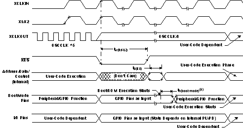
Table 5-6 Reset (XRS) Timing Requirements
| MIN | NOM | MAX | UNIT | ||||
|---|---|---|---|---|---|---|---|
| tw(RSL1)(1) | Pulse duration, stable input clock to XRS high | 64tc(OSCCLK) | cycles | ||||
| tw(RSL2) | Pulse duration, XRS low | Warm reset | 64tc(OSCCLK) | cycles | |||
| tw(WDRS) | Pulse duration, reset pulse generated by watchdog | 512tc(OSCCLK) | cycles | ||||
| td(EX) | Delay time, address/data valid after XRS high | 32tc(OSCCLK) | cycles | ||||
| tOSCST(2) | Oscillator start-up time | 1 | 10 | ms | |||
| th(boot-mode) | Hold time for boot-mode pins | 200tc(OSCCLK) | cycles | ||||
| tpup | Power-up time | 5 | ms | ||||
(1) In addition to the tw(RSL1) requirement, XRS must be low until VDD has reached the minimum operating voltage.
(2) Dependent on crystal/resonator and board design.

A. After reset, the Boot ROM code samples BOOT Mode pins. Based on the status of the Boot Mode pin, the boot code branches to destination memory or boot code function. If Boot ROM code executes after power-on conditions (in debugger environment), the Boot code execution time is based on the current SYSCLKOUT speed. The SYSCLKOUT will be based on user environment and could be with or without PLL enabled.
Figure 5-4 Warm Reset Figure 5-5 shows an example for the effect of writing into PLLCR register. In the first phase, PLLCR = 0x0003 and SYSCLKOUT = OSCCLK × 2. The PLLCR is then written with 0x0007 (setting for OSCCLK × 8). Right after the PLLCR register is written, the PLL lock-up phase begins. During this phase, SYSCLKOUT = OSCCLK/2. After the PLL lock-up is complete (which takes 2600 OSCCLK cycles), SYSCLKOUT reflects the new operating frequency, OSCCLK × 4.
 Figure 5-5 Example of Effect of Writing Into PLLCR Register