JAJSDV6F November 2009 – January 2017 TMS320C6746
PRODUCTION DATA.
- 1デバイスの概要
- 2Revision History
-
3Device Comparison
- 3.1 Device Characteristics
- 3.2 Device Compatibility
- 3.3 DSP Subsystem
- 3.4 Memory Map Summary
- 3.5 Pin Assignments
- 3.6 Pin Multiplexing Control
- 3.7
Terminal Functions
- 3.7.1 Device Reset, NMI and JTAG
- 3.7.2 High-Frequency Oscillator and PLL
- 3.7.3 Real-Time Clock and 32-kHz Oscillator
- 3.7.4 DEEPSLEEP Power Control
- 3.7.5 External Memory Interface A (EMIFA)
- 3.7.6 DDR2/mDDR Controller
- 3.7.7 Serial Peripheral Interface Modules (SPI)
- 3.7.8 Programmable Real-Time Unit (PRU)
- 3.7.9 Enhanced Capture/Auxiliary PWM Modules (eCAP0)
- 3.7.10 Enhanced Pulse Width Modulators (eHRPWM)
- 3.7.11 Boot
- 3.7.12 Universal Asynchronous Receiver/Transmitters (UART0, UART1, UART2)
- 3.7.13 Inter-Integrated Circuit Modules(I2C0, I2C1)
- 3.7.14 Timers
- 3.7.15 Multichannel Audio Serial Ports (McASP)
- 3.7.16 Multichannel Buffered Serial Ports (McBSP)
- 3.7.17 Universal Serial Bus Modules (USB0)
- 3.7.18 Ethernet Media Access Controller (EMAC)
- 3.7.19 Multimedia Card/Secure Digital (MMC/SD)
- 3.7.20 Universal Host-Port Interface (UHPI)
- 3.7.21 Universal Parallel Port (uPP)
- 3.7.22 Video Port Interface (VPIF)
- 3.7.23 General Purpose Input Output
- 3.7.24 Reserved and No Connect
- 3.7.25 Supply and Ground
- 3.8 Unused Pin Configurations
- 4Device Configuration
-
5Specifications
- 5.1 Absolute Maximum Ratings Over Operating Junction Temperature Range (Unless Otherwise Noted)
- 5.2 Handling Ratings
- 5.3 Recommended Operating Conditions
- 5.4 Notes on Recommended Power-On Hours (POH)
- 5.5 Electrical Characteristics Over Recommended Ranges of Supply Voltage and Operating Junction Temperature (Unless Otherwise Noted)
-
6Peripheral Information and Electrical Specifications
- 6.1 Parameter Information
- 6.2 Recommended Clock and Control Signal Transition Behavior
- 6.3 Power Supplies
- 6.4 Reset
- 6.5 Crystal Oscillator or External Clock Input
- 6.6 Clock PLLs
- 6.7 Interrupts
- 6.8 Power and Sleep Controller (PSC)
- 6.9 Enhanced Direct Memory Access Controller (EDMA3)
- 6.10 External Memory Interface A (EMIFA)
- 6.11
DDR2/mDDR Memory Controller
- 6.11.1 DDR2/mDDR Memory Controller Electrical Data/Timing
- 6.11.2 DDR2/mDDR Memory Controller Register Description(s)
- 6.11.3
DDR2/mDDR Interface
- 6.11.3.1 DDR2/mDDR Interface Schematic
- 6.11.3.2 Compatible JEDEC DDR2/mDDR Devices
- 6.11.3.3 PCB Stackup
- 6.11.3.4 Placement
- 6.11.3.5 DDR2/mDDR Keep Out Region
- 6.11.3.6 Bulk Bypass Capacitors
- 6.11.3.7 High-Speed Bypass Capacitors
- 6.11.3.8 Net Classes
- 6.11.3.9 DDR2/mDDR Signal Termination
- 6.11.3.10 VREF Routing
- 6.11.3.11 DDR2/mDDR CK and ADDR_CTRL Routing
- 6.11.3.12 DDR2/mDDR Boundary Scan Limitations
- 6.12 Memory Protection Units
- 6.13 MMC / SD / SDIO (MMCSD0, MMCSD1)
- 6.14 Multichannel Audio Serial Port (McASP)
- 6.15
Multichannel Buffered Serial Port (McBSP)
- 6.15.1 McBSP Peripheral Register Description(s)
- 6.15.2
McBSP Electrical Data/Timing
- 6.15.2.1
Multichannel Buffered Serial Port (McBSP) Timing
- Table 6-50 Timing Requirements for McBSP0 [1.3V, 1.2V, 1.1V] (see )
- Table 6-51 Timing Requirements for McBSP0 [1.0V] (see )
- Table 6-52 Switching Characteristics for McBSP0 [1.3V, 1.2V, 1.1V] (see )
- Table 6-53 Switching Characteristics for McBSP0 [1.0V] (see )
- Table 6-54 Timing Requirements for McBSP1 [1.3V, 1.2V, 1.1V] (see )
- Table 6-55 Timing Requirements for McBSP1 [1.0V] (see )
- Table 6-56 Switching Characteristics for McBSP1 [1.3V, 1.2V, 1.1V] (see )
- Table 6-57 Switching Characteristics for McBSP1 [1.0V] (see )
- Table 6-58 Timing Requirements for McBSP0 FSR When GSYNC = 1 (see )
- Table 6-59 Timing Requirements for McBSP1 FSR When GSYNC = 1 (see )
- 6.15.2.1
Multichannel Buffered Serial Port (McBSP) Timing
- 6.16
Serial Peripheral Interface Ports (SPI0, SPI1)
- 6.16.1 SPI Peripheral Registers Description(s)
- 6.16.2
SPI Electrical Data/Timing
- 6.16.2.1
Serial Peripheral Interface (SPI) Timing
- Table 6-61 General Timing Requirements for SPI0 Master Modes
- Table 6-62 General Timing Requirements for SPI0 Slave Modes
- Table 6-69 General Timing Requirements for SPI1 Master Modes
- Table 6-70 General Timing Requirements for SPI1 Slave Modes
- Table 6-71 Additional SPI1 Master Timings, 4-Pin Enable Option
- Table 6-72 Additional SPI1 Master Timings, 4-Pin Chip Select Option
- 6.16.2.1
Serial Peripheral Interface (SPI) Timing
- 6.17 Inter-Integrated Circuit Serial Ports (I2C)
- 6.18 Universal Asynchronous Receiver/Transmitter (UART)
- 6.19 Universal Serial Bus OTG Controller (USB0) [USB2.0 OTG]
- 6.20 Ethernet Media Access Controller (EMAC)
- 6.21 Management Data Input/Output (MDIO)
- 6.22 Host-Port Interface (UHPI)
- 6.23 Universal Parallel Port (uPP)
- 6.24 Video Port Interface (VPIF)
- 6.25 Enhanced Capture (eCAP) Peripheral
- 6.26 Enhanced High-Resolution Pulse-Width Modulator (eHRPWM)
- 6.27 Timers
- 6.28 Real Time Clock (RTC)
- 6.29 General-Purpose Input/Output (GPIO)
- 6.30 Programmable Real-Time Unit Subsystem (PRUSS)
- 6.31 Emulation Logic
- 7Device and Documentation Support
- 8Mechanical Packaging and Orderable Information
パッケージ・オプション
デバイスごとのパッケージ図は、PDF版データシートをご参照ください。
メカニカル・データ(パッケージ|ピン)
- ZCE|361
- ZWT|361
サーマルパッド・メカニカル・データ
発注情報
6.10.4 EMIFA Connection Examples
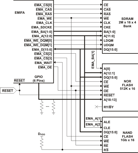
Figure 6-10 illustrates an example of how SDRAM, NOR, and NAND flash devices might be connected to EMIFA simultaneously. The SDRAM chip select must be EMA_CS[0]. Note that the NOR flash is connected to EMA_CS[2] and the NAND flash is connected to EMA_CS[3] in this example. Note that any type of asynchronous memory may be connected to EMA_CS[5:2].
The on-chip bootloader makes some assumptions on which chip select the contains the boot image, and this depends on the boot mode. For NOR boot mode; the on-chip bootloader requires that the image be stored in NOR flash on EMA_CS[2]. For NAND boot mode, the bootloader requires that the boot image is stored in NAND flash on EMA_CS[3]. It is always possible to have the image span multiple chip selects, but this must be supported by second stage boot code stored in the external flash.
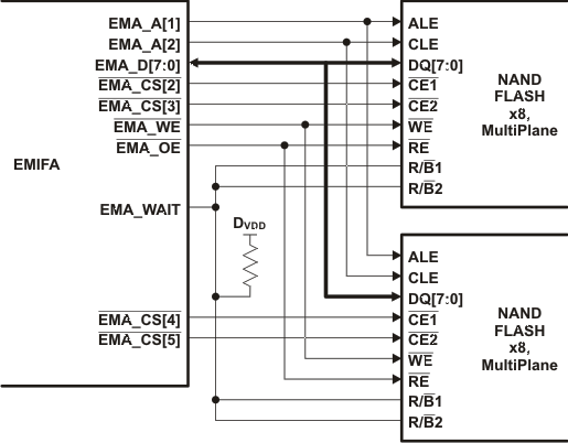
A likely use case with more than one EMIFA chip select used for NAND flash is illustrated in Figure 6-11. This figure shows how two multiplane NAND flash devices with two chip selects each would connect to the EMIFA. In this case if NAND is the boot memory, then the boot image needs to be stored in the NAND area selected by EMA_CS[3]. Part of the application image could spill over into the NAND regions selected by other EMIFA chip selects; but would rely on the code stored in the EMA_CS[3] area to bootload it.
 Figure 6-10 Connection Diagram: SDRAM, NOR, NAND
 Figure 6-11 EMIFA Connection Diagram: Multiple NAND Flash Planes