SPRS357D August 2006 – June 2020 TMS320F28044
PRODUCTION DATA.
- 1Device Overview
- 2Revision History
- 3Device Comparison
- 4Terminal Configuration and Functions
-
5Specifications
- 5.1 Absolute Maximum Ratings
- 5.2 ESD Ratings – Commercial
- 5.3 Recommended Operating Conditions
- 5.4 Power Consumption Summary
- 5.5 Electrical Characteristics
- 5.6 Thermal Resistance Characteristics for F28044 100-Ball GGM Package
- 5.7 Thermal Resistance Characteristics for F28044 100-Pin PZ Package
- 5.8 Thermal Design Considerations
- 5.9
Timing and Switching Characteristics
- 5.9.1 Timing Parameter Symbology
- 5.9.2 Power Sequencing
- 5.9.3 Clock Requirements and Characteristics
- 5.9.4
Peripherals
- 5.9.4.1 General-Purpose Input/Output (GPIO)
- 5.9.4.2 Enhanced Control Peripherals
- 5.9.4.3 External Interrupt Timing
- 5.9.4.4 I2C Electrical Specification and Timing
- 5.9.4.5 Serial Peripheral Interface (SPI) Master Mode Timing
- 5.9.4.6 SPI Slave Mode Timing
- 5.9.5 JTAG Debug Probe Connection Without Signal Buffering for the DSP
- 5.9.6 Flash Timing
- 5.10 On-Chip Analog-to-Digital Converter
-
6Detailed Description
- 6.1
Brief Descriptions
- 6.1.1 C28x CPU
- 6.1.2 Memory Bus (Harvard Bus Architecture)
- 6.1.3 Peripheral Bus
- 6.1.4 Real-Time JTAG and Analysis
- 6.1.5 Flash
- 6.1.6 M0, M1 SARAMs
- 6.1.7 L0, L1 SARAMs
- 6.1.8 Boot ROM
- 6.1.9 Security
- 6.1.10 Peripheral Interrupt Expansion (PIE) Block
- 6.1.11 External Interrupts (XINT1, XINT2, XNMI)
- 6.1.12 Oscillator and PLL
- 6.1.13 Watchdog
- 6.1.14 Peripheral Clocking
- 6.1.15 Low-Power Modes
- 6.1.16 Peripheral Frames 0, 1, 2 (PFn)
- 6.1.17 General-Purpose Input/Output (GPIO) Multiplexer
- 6.1.18 32-Bit CPU-Timers (0, 1, 2)
- 6.1.19 Control Peripherals
- 6.1.20 Serial Port Peripherals
- 6.2
Peripherals
- 6.2.1 32-Bit CPU-Timers 0/1/2
- 6.2.2 Enhanced PWM Modules (ePWM1–16)
- 6.2.3 Hi-Resolution PWM (HRPWM)
- 6.2.4 Enhanced Analog-to-Digital Converter (ADC) Module
- 6.2.5 Serial Communications Interface (SCI) Module (SCI-A)
- 6.2.6 Serial Peripheral Interface (SPI) Module (SPI-A)
- 6.2.7 Inter-Integrated Circuit (I2C)
- 6.2.8 GPIO MUX
- 6.3 Memory Map
- 6.4 Register Map
- 6.5 Interrupts
- 6.6 System Control
- 6.7 Low-Power Modes Block
- 6.1
Brief Descriptions
- 7Applications, Implementation, and Layout
- 8Device and Documentation Support
- 9Mechanical, Packaging, and Orderable Information
パッケージ・オプション
デバイスごとのパッケージ図は、PDF版データシートをご参照ください。
メカニカル・データ(パッケージ|ピン)
- PZ|100
サーマルパッド・メカニカル・データ
- PZ|100
発注情報
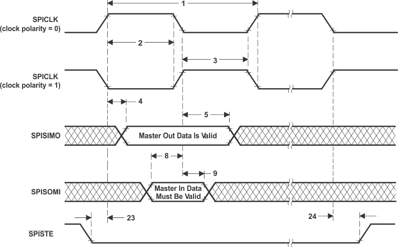
Table 5-26 SPI Master Mode External Timing (Clock Phase = 0)(1)(2)(3)(4)(5)
| NO. | PARAMETER | BRR EVEN | BRR ODD | UNIT | |||
|---|---|---|---|---|---|---|---|
| MIN | MAX | MIN | MAX | ||||
| 1 | tc(SPC)M | Cycle time, SPICLK | 4tc(LSPCLK) | 128tc(LSPCLK) | 5tc(LSPCLK) | 127tc(LSPCLK) | ns |
| 2 | tw(SPC1)M | Pulse duration, SPICLK first pulse | 0.5tc(SPC)M – 10 | 0.5tc(SPC)M + 10 | 0.5tc(SPC)M + 0.5tc(LSPCLK) – 10 | 0.5tc(SPC)M +
0.5tc(LSPCLK) + 10 |
ns |
| 3 | tw(SPC2)M | Pulse duration, SPICLK second pulse | 0.5tc(SPC)M – 10 | 0.5tc(SPC)M + 10 | 0.5tc(SPC)M – 0.5tc(LSPCLK) – 10 | 0.5tc(SPC)M –
0.5tc(LSPCLK) + 10 |
ns |
| 4 | td(SIMO)M | Delay time, SPICLK to SPISIMO valid | 10 | 10 | ns | ||
| 5 | tv(SIMO)M | Valid time, SPISIMO valid after SPICLK | 0.5tc(SPC)M – 10 | 0.5tc(SPC)M – 0.5tc(LSPCLK) – 10 | ns | ||
| 8 | tsu(SOMI)M | Setup time, SPISOMI before SPICLK | 35 | 35 | ns | ||
| 9 | th(SOMI)M | Hold time, SPISOMI valid after SPICLK | 0 | 0 | ns | ||
| 23 | td(SPC)M | Delay time, SPISTE active to SPICLK | tc(SPC)M – 10 | 0.5tc(SPC)M – 0.5tc(LSPCLK) – 10 | ns | ||
| 24 | td(STE)M | Delay time, SPICLK to SPISTE inactive | 0.5tc(SPC)M – 10 | 0.5tc(SPC)M – 0.5tc(LSPCLK) – 10 | ns | ||
(1) The MASTER / SLAVE bit (SPICTL.2) is set and the CLOCK PHASE bit (SPICTL.3) is cleared.
(2) tc(SPC) = SPI clock cycle time = LSPCLK/4 or LSPCLK/(SPIBRR +1)
(3) tc(LCO) = LSPCLK cycle time
(4) Internal clock prescalers must be adjusted such that the SPI clock speed is limited to the following SPI clock rate:
Master mode transmit 25-MHz MAX, master mode receive 12.5-MHz MAX
Slave mode transmit 12.5-MAX, slave mode receive 12.5-MHz MAX.
Master mode transmit 25-MHz MAX, master mode receive 12.5-MHz MAX
Slave mode transmit 12.5-MAX, slave mode receive 12.5-MHz MAX.
(5) The active edge of the SPICLK signal referenced is controlled by the clock polarity bit (SPICCR.6).
 Figure 5-15 SPI Master Mode External Timing (Clock Phase = 0)