JAJSFH1J November 2010 – September 2021 TMS320F28062 , TMS320F28062F , TMS320F28063 , TMS320F28064 , TMS320F28065 , TMS320F28066 , TMS320F28067 , TMS320F28068F , TMS320F28068M , TMS320F28069 , TMS320F28069F , TMS320F28069M
PRODUCTION DATA
- 1 特長
- 2 アプリケーション
- 3 概要
- 4 Revision History
- 5 Device Comparison
- 6 Terminal Configuration and Functions
-
7 Specifications
- 7.1 Absolute Maximum Ratings
- 7.2 ESD Ratings – Commercial
- 7.3 ESD Ratings – Automotive
- 7.4 Recommended Operating Conditions
- 7.5 Power Consumption Summary
- 7.6 Electrical Characteristics
- 7.7 Thermal Resistance Characteristics
- 7.8 Thermal Design Considerations
- 7.9 Debug Probe Connection Without Signal Buffering for the MCU
- 7.10 Parameter Information
- 7.11 Test Load Circuit
- 7.12 Power Sequencing
- 7.13 Clock Specifications
- 7.14 Flash Timing
-
8 Detailed Description
- 8.1
Overview
- 8.1.1 CPU
- 8.1.2 Control Law Accelerator (CLA)
- 8.1.3 Viterbi, Complex Math, CRC Unit (VCU)
- 8.1.4 Memory Bus (Harvard Bus Architecture)
- 8.1.5 Peripheral Bus
- 8.1.6 Real-Time JTAG and Analysis
- 8.1.7 Flash
- 8.1.8 M0, M1 SARAMs
- 8.1.9 L4 SARAM, and L0, L1, L2, L3, L5, L6, L7, and L8 DPSARAMs
- 8.1.10 Boot ROM
- 8.1.11 Security
- 8.1.12 Peripheral Interrupt Expansion (PIE) Block
- 8.1.13 External Interrupts (XINT1 to XINT3)
- 8.1.14 Internal Zero Pin Oscillators, Oscillator, and PLL
- 8.1.15 Watchdog
- 8.1.16 Peripheral Clocking
- 8.1.17 Low-power Modes
- 8.1.18 Peripheral Frames 0, 1, 2, 3 (PFn)
- 8.1.19 General-Purpose Input/Output (GPIO) Multiplexer
- 8.1.20 32-Bit CPU-Timers (0, 1, 2)
- 8.1.21 Control Peripherals
- 8.1.22 Serial Port Peripherals
- 8.2 Memory Maps
- 8.3 Register Maps
- 8.4 Device Debug Registers
- 8.5 VREG, BOR, POR
- 8.6 System Control
- 8.7 Low-power Modes Block
- 8.8 Interrupts
- 8.9
Peripherals
- 8.9.1 CLA Overview
- 8.9.2 Analog Block
- 8.9.3 Detailed Descriptions
- 8.9.4 Serial Peripheral Interface (SPI) Module
- 8.9.5 Serial Communications Interface (SCI) Module
- 8.9.6
Multichannel Buffered Serial Port (McBSP) Module
- 8.9.6.1
McBSP Electrical Data/Timing
- 8.9.6.1.1 McBSP Transmit and Receive Timing
- 8.9.6.1.2
McBSP as SPI Master or Slave Timing
- 8.9.6.1.2.1 McBSP as SPI Master or Slave Timing Requirements (CLKSTP = 10b, CLKXP = 0)
- 8.9.6.1.2.2 McBSP as SPI Master or Slave Switching Characteristics (CLKSTP = 10b, CLKXP = 0)
- 8.9.6.1.2.3 McBSP as SPI Master or Slave Timing Requirements (CLKSTP = 11b, CLKXP = 0)
- 8.9.6.1.2.4 McBSP as SPI Master or Slave Switching Characteristics (CLKSTP = 11b, CLKXP = 0)
- 8.9.6.1.2.5 McBSP as SPI Master or Slave Timing Requirements (CLKSTP = 10b, CLKXP = 1)
- 8.9.6.1.2.6 McBSP as SPI Master or Slave Switching Characteristics (CLKSTP = 10b, CLKXP = 1)
- 8.9.6.1.2.7 McBSP as SPI Master or Slave Timing Requirements (CLKSTP = 11b, CLKXP = 1)
- 8.9.6.1.2.8 McBSP as SPI Master or Slave Switching Characteristics (CLKSTP = 11b, CLKXP = 1)
- 8.9.6.1
McBSP Electrical Data/Timing
- 8.9.7 Enhanced Controller Area Network (eCAN) Module
- 8.9.8 Inter-Integrated Circuit (I2C)
- 8.9.9 Enhanced Pulse Width Modulator (ePWM) Modules (ePWM1 to ePWM8)
- 8.9.10 High-Resolution PWM (HRPWM)
- 8.9.11 Enhanced Capture Module (eCAP1)
- 8.9.12 High-Resolution Capture Modules (HRCAP1 to HRCAP4)
- 8.9.13 Enhanced Quadrature Encoder Modules (eQEP1, eQEP2)
- 8.9.14 JTAG Port
- 8.9.15 General-Purpose Input/Output (GPIO) MUX
- 8.9.16 Universal Serial Bus (USB)
- 8.1
Overview
- 9 Applications, Implementation, and Layout
- 10Device and Documentation Support
- 11Mechanical, Packaging, and Orderable Information
パッケージ・オプション
メカニカル・データ(パッケージ|ピン)
- PZ|100
サーマルパッド・メカニカル・データ
- PZ|100
発注情報
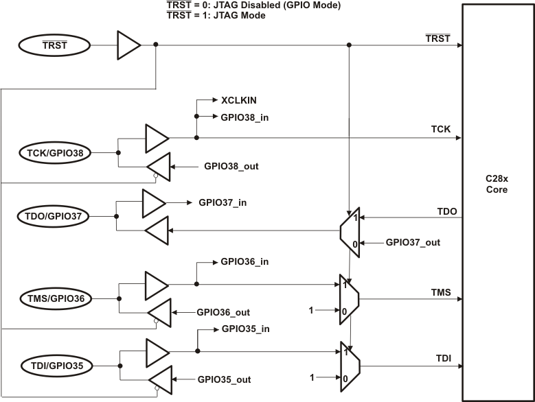
8.9.14 JTAG Port
On the 2806x device, the JTAG port is reduced to five pins ( TRST, TCK, TDI, TMS, TDO). TCK, TDI, TMS, and TDO pins are also GPIO pins. The TRST signal selects either JTAG or GPIO operating mode for the pins in Figure 8-54. During debug, the GPIO function of these pins are not available. If the GPIO38/TCK/XCLKIN pin is used to provide an external clock, an alternate clock source should be used to clock the device during debug because this pin will be needed for the TCK function.
In 2806x devices, the JTAG pins may also be used as GPIO pins. Care should be taken in the board design to ensure that the circuitry connected to these pins do not affect the debug capabilities of the JTAG pin function. Any circuitry connected to these pins should not prevent the debug probe from driving (or being driven by) the JTAG pins for successful debug.
 Figure 8-54 JTAG/GPIO Multiplexing