JAJSEG7 December 2017 TMS320F28377D-EP
PRODUCTION DATA.
- 1デバイスの概要
- 2改訂履歴
- 3Terminal Configuration and Functions
-
4Specifications
- 4.1 Absolute Maximum Ratings
- 4.2 ESD Ratings
- 4.3 Recommended Operating Conditions
- 4.4 Power Consumption Summary
- 4.5 Electrical Characteristics
- 4.6 Thermal Resistance Characteristics
- 4.7
System
- 4.7.1 Power Sequencing
- 4.7.2 Reset Timing
- 4.7.3
Clock Specifications
- 4.7.3.1 Clock Sources
- 4.7.3.2 Clock Frequencies, Requirements, and Characteristics
- 4.7.3.3 Input Clocks and PLLs
- 4.7.3.4 Crystal Oscillator
- 4.7.3.5 Internal Oscillators
- 4.7.4 Flash Parameters
- 4.7.5 Emulation/JTAG
- 4.7.6 GPIO Electrical Data and Timing
- 4.7.7 Interrupts
- 4.7.8
Low-Power Modes
- 4.7.8.1 Clock-Gating Low-Power Modes
- 4.7.8.2 Power-Gating Low-Power Modes
- 4.7.8.3
Low-Power Mode Wakeup Timing
- Table 4-29 IDLE Mode Timing Requirements
- Table 4-30 IDLE Mode Switching Characteristics
- Table 4-31 STANDBY Mode Timing Requirements
- Table 4-32 STANDBY Mode Switching Characteristics
- Table 4-33 HALT Mode Timing Requirements
- Table 4-34 HALT Mode Switching Characteristics
- Table 4-35 HIBERNATE Mode Timing Requirements
- Table 4-36 HIBERNATE Mode Switching Characteristics
- 4.7.9 External Memory Interface (EMIF)
- 4.8
Analog Peripherals
- 4.8.1
Analog-to-Digital Converter (ADC)
- 4.8.1.1
ADC Electrical Data and Timing
- Table 4-41 ADC Operating Conditions (16-Bit Differential Mode)
- Table 4-42 ADC Characteristics (16-Bit Differential Mode)
- Table 4-43 ADC Operating Conditions (12-Bit Single-Ended Mode)
- Table 4-44 ADC Characteristics (12-Bit Single-Ended Mode)
- Table 4-45 ADCEXTSOC Timing Requirements
- 4.8.1.1.1 ADC Input Models
- 4.8.1.1.2 ADC Timing Diagrams
- 4.8.1.2 Temperature Sensor Electrical Data and Timing
- 4.8.1.1
ADC Electrical Data and Timing
- 4.8.2 Comparator Subsystem (CMPSS)
- 4.8.3 Buffered Digital-to-Analog Converter (DAC)
- 4.8.1
Analog-to-Digital Converter (ADC)
- 4.9
Control Peripherals
- 4.9.1 Enhanced Capture (eCAP)
- 4.9.2 Enhanced Pulse Width Modulator (ePWM)
- 4.9.3 Enhanced Quadrature Encoder Pulse (eQEP)
- 4.9.4 High-Resolution Pulse Width Modulator (HRPWM)
- 4.9.5 Sigma-Delta Filter Module (SDFM)
- 4.10
Communications Peripherals
- 4.10.1 Controller Area Network (CAN)
- 4.10.2 Inter-Integrated Circuit (I2C)
- 4.10.3
Multichannel Buffered Serial Port (McBSP)
- 4.10.3.1
McBSP Electrical Data and Timing
- 4.10.3.1.1 McBSP Transmit and Receive Timing
- 4.10.3.1.2
McBSP as SPI Master or Slave Timing
- Table 4-69 McBSP as SPI Master or Slave Timing Requirements (CLKSTP = 10b, CLKXP = 0)
- Table 4-70 McBSP as SPI Master or Slave Switching Characteristics (CLKSTP = 10b, CLKXP = 0)
- Table 4-71 McBSP as SPI Master or Slave Timing Requirements (CLKSTP = 11b, CLKXP = 0)
- Table 4-72 McBSP as SPI Master or Slave Switching Characteristics (CLKSTP = 11b, CLKXP = 0)
- Table 4-73 McBSP as SPI Master or Slave Timing Requirements (CLKSTP = 10b, CLKXP = 1)
- Table 4-74 McBSP as SPI Master or Slave Switching Characteristics (CLKSTP = 10b, CLKXP = 1)
- Table 4-75 McBSP as SPI Master or Slave Timing Requirements (CLKSTP = 11b, CLKXP = 1)
- Table 4-76 McBSP as SPI Master or Slave Switching Characteristics (CLKSTP = 11b, CLKXP = 1)
- 4.10.3.1
McBSP Electrical Data and Timing
- 4.10.4 Serial Communications Interface (SCI)
- 4.10.5 Serial Peripheral Interface (SPI)
- 4.10.6 Universal Serial Bus (USB) Controller
- 4.10.7 Universal Parallel Port (uPP) Interface
-
5Detailed Description
- 5.1 Overview
- 5.2 Functional Block Diagram
- 5.3 Memory
- 5.4 Identification
- 5.5 Bus Architecture – Peripheral Connectivity
- 5.6 C28x Processor
- 5.7 Control Law Accelerator
- 5.8 Direct Memory Access
- 5.9 Interprocessor Communication Module
- 5.10 Boot ROM and Peripheral Booting
- 5.11 Dual Code Security Module
- 5.12 Timers
- 5.13 Nonmaskable Interrupt With Watchdog Timer (NMIWD)
- 5.14 Watchdog
- 5.15 Configurable Logic Block (CLB)
- 6Applications, Implementation, and Layout
- 7デバイスおよびドキュメントのサポート
- 8メカニカル、パッケージ、および注文情報
パッケージ・オプション
メカニカル・データ(パッケージ|ピン)
サーマルパッド・メカニカル・データ
- PTP|176
発注情報
4.7.5 Emulation/JTAG
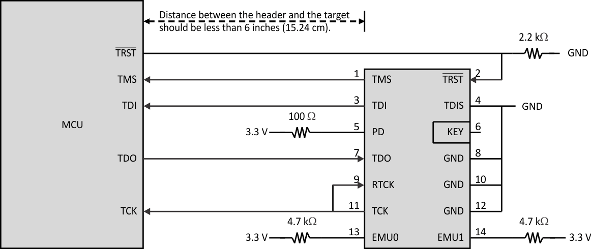
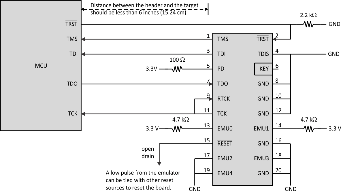
The JTAG port has five dedicated pins: TRST, TMS, TDI, TDO, and TCK. The TRST signal should always be pulled down through a 2.2-kΩ pulldown resistor on the board. This MCU does not support the EMU0 and EMU1 signals that are present on 14-pin and 20-pin emulation headers. These signals should always be pulled up at the emulation header through a pair of board pullup resistors ranging from 2.2 kΩ to 4.7 kΩ (depending on the drive strength of the debugger ports). Typically, a 2.2-kΩ value is used.
See Figure 4-10 to see how the 14-pin JTAG header connects to the MCU’s JTAG port signals. Figure 4-11 shows how to connect to the 20-pin header. The 20-pin JTAG header terminals EMU2, EMU3, and EMU4 are not used and should be grounded.
The PD (Power Detect) terminal of the emulator header should be connected to the board 3.3-V supply. Header GND terminals should be connected to board ground. TDIS (Cable Disconnect Sense) should also be connected to board ground. The JTAG clock should be looped from the header TCK output terminal back to the RTCK input terminal of the header (to sense clock continuity by the emulator). Header terminal RESET is an open-drain output from the emulator header that enables board components to be reset through emulator commands (available only through the 20-pin header).
Typically, no buffers are needed on the JTAG signals when the distance between the MCU target and the JTAG header is smaller than 6 in (15.24 cm), and no other devices are present on the JTAG chain. Otherwise, each signal should be buffered. Additionally, for most emulator operations at 10 MHz, no series resistors are needed on the JTAG signals. However, if high emulation speeds are expected (35 MHz or so), 22-Ω resistors should be placed in series on each JTAG signal.
For more information about hardware breakpoints and watchpoints, see Hardware Breakpoints and Watchpoints for C28x in CCS.
For more information about JTAG emulation, see the XDS Target Connection Guide.
 Figure 4-10 Connecting to the 14-Pin JTAG Header
 Figure 4-11 Connecting to the 20-Pin JTAG Header