SPRSP69B July   2023  – November 2023 TMS320F28P650DK , TMS320F28P659DK-Q1

PRODMIX  

  1.   1
  2. Features
  3. Applications
  4. Description
    1. 3.1 Functional Block Diagram
  5. Device Comparison
    1. 4.1 Related Products
  6. Pin Configuration and Functions
    1. 5.1 Pin Diagrams
    2. 5.2 Pin Attributes
    3. 5.3 Signal Descriptions
      1. 5.3.1 Analog Signals
      2. 5.3.2 Digital Signals
      3. 5.3.3 Power and Ground
      4. 5.3.4 Test, JTAG, and Reset
    4. 5.4 Pins With Internal Pullup and Pulldown
    5. 5.5 Pin Multiplexing
      1. 5.5.1 GPIO Muxed Pins
      2. 5.5.2 USB Pin Muxing
      3. 5.5.3 High-Speed SPI Pin Muxing
    6. 5.6 Connections for Unused Pins
  7. Specifications
    1. 6.1  Absolute Maximum Ratings
    2. 6.2  ESD Ratings – Commercial
    3. 6.3  ESD Ratings – Automotive
    4. 6.4  Recommended Operating Conditions
    5. 6.5  Power Consumption Summary
      1. 6.5.1 System Current Consumption VREG Enabled
      2. 6.5.2 System Current Consumption VREG Disable - External Supply
      3. 6.5.3 Operating Mode Test Description
      4. 6.5.4 Current Consumption Graphs
      5. 6.5.5 Reducing Current Consumption
        1. 6.5.5.1 Typical Current Reduction per Disabled Peripheral
    6. 6.6  Electrical Characteristics
    7. 6.7  Thermal Resistance Characteristics for ZEJ Package
    8. 6.8  Thermal Resistance Characteristics for PTP Package
    9. 6.9  Thermal Resistance Characteristics for NMR Package
    10. 6.10 Thermal Resistance Characteristics for PZP Package
    11. 6.11 Thermal Design Considerations
    12. 6.12 System
      1. 6.12.1  Power Management Module (PMM)
        1. 6.12.1.1 Introduction
        2. 6.12.1.2 Overview
          1. 6.12.1.2.1 Power Rail Monitors
            1. 6.12.1.2.1.1 I/O POR (Power-On Reset) Monitor
            2. 6.12.1.2.1.2 I/O BOR (Brown-Out Reset) Monitor
            3. 6.12.1.2.1.3 VDD POR (Power-On Reset) Monitor
          2. 6.12.1.2.2 External Supervisor Usage
          3. 6.12.1.2.3 Delay Blocks
          4. 6.12.1.2.4 Internal 1.2-V LDO Voltage Regulator (VREG)
          5. 6.12.1.2.5 VREGENZ
        3. 6.12.1.3 External Components
          1. 6.12.1.3.1 Decoupling Capacitors
            1. 6.12.1.3.1.1 VDDIO Decoupling
            2. 6.12.1.3.1.2 VDD Decoupling
        4. 6.12.1.4 Power Sequencing
          1. 6.12.1.4.1 Supply Pins Ganging
          2. 6.12.1.4.2 Signal Pins Power Sequence
          3. 6.12.1.4.3 Supply Pins Power Sequence
            1. 6.12.1.4.3.1 External VREG/VDD Mode Sequence
            2. 6.12.1.4.3.2 Internal VREG/VDD Mode Sequence
            3. 6.12.1.4.3.3 Supply Sequencing Summary and Effects of Violations
            4. 6.12.1.4.3.4 Supply Slew Rate
        5. 6.12.1.5 Power Management Module Electrical Data and Timing
          1. 6.12.1.5.1 Power Management Module Operating Conditions
          2. 6.12.1.5.2 Power Management Module Characteristics
      2. 6.12.2  Reset Timing
        1. 6.12.2.1 Reset Sources
        2. 6.12.2.2 Reset Electrical Data and Timing
          1. 6.12.2.2.1 Reset XRSn Timing Requirements
          2. 6.12.2.2.2 Reset XRSn Switching Characteristics
          3. 6.12.2.2.3 Reset Timing Diagrams
      3. 6.12.3  Clock Specifications
        1. 6.12.3.1 Clock Sources
        2. 6.12.3.2 Clock Frequencies, Requirements, and Characteristics
          1. 6.12.3.2.1 Input Clock Frequency and Timing Requirements, PLL Lock Times
            1. 6.12.3.2.1.1 Input Clock Frequency
            2. 6.12.3.2.1.2 XTAL Oscillator Characteristics
            3. 6.12.3.2.1.3 X1 Input Level Characteristics When Using an External Clock Source Not a Crystal
            4. 6.12.3.2.1.4 X1 Timing Requirements
            5. 6.12.3.2.1.5 AUXCLKIN Timing Requirements
            6. 6.12.3.2.1.6 APLL Characteristics
            7. 6.12.3.2.1.7 XCLKOUT Switching Characteristics PLL Bypassed or Enabled
            8. 6.12.3.2.1.8 Internal Clock Frequencies
        3. 6.12.3.3 Input Clocks
        4. 6.12.3.4 XTAL Oscillator
          1. 6.12.3.4.1 Introduction
          2. 6.12.3.4.2 Overview
            1. 6.12.3.4.2.1 Electrical Oscillator
              1. 6.12.3.4.2.1.1 Modes of Operation
                1. 6.12.3.4.2.1.1.1 Crystal Mode of Operation
                2. 6.12.3.4.2.1.1.2 Single-Ended Mode of Operation
              2. 6.12.3.4.2.1.2 XTAL Output on XCLKOUT
            2. 6.12.3.4.2.2 Quartz Crystal
            3. 6.12.3.4.2.3 GPIO Modes of Operation
          3. 6.12.3.4.3 Functional Operation
            1. 6.12.3.4.3.1 ESR – Effective Series Resistance
            2. 6.12.3.4.3.2 Rneg – Negative Resistance
            3. 6.12.3.4.3.3 Start-up Time
            4. 6.12.3.4.3.4 DL – Drive Level
          4. 6.12.3.4.4 How to Choose a Crystal
          5. 6.12.3.4.5 Testing
          6. 6.12.3.4.6 Common Problems and Debug Tips
          7. 6.12.3.4.7 Crystal Oscillator Specifications
            1. 6.12.3.4.7.1 Crystal Oscillator Electrical Characteristics
            2. 6.12.3.4.7.2 Crystal Equivalent Series Resistance (ESR) Requirements
            3. 6.12.3.4.7.3 Crystal Oscillator Parameters
            4. 6.12.3.4.7.4 Crystal Oscillator Electrical Characteristics
        5. 6.12.3.5 Internal Oscillators
          1. 6.12.3.5.1 INTOSC Characteristics
      4. 6.12.4  Flash Parameters
        1. 6.12.4.1 Flash Parameters 
      5. 6.12.5  RAM Specifications
      6. 6.12.6  ROM Specifications
      7. 6.12.7  Emulation/JTAG
        1. 6.12.7.1 JTAG Electrical Data and Timing
          1. 6.12.7.1.1 JTAG Timing Requirements
          2. 6.12.7.1.2 JTAG Switching Characteristics
          3. 6.12.7.1.3 JTAG Timing Diagram
        2. 6.12.7.2 cJTAG Electrical Data and Timing
          1. 6.12.7.2.1 cJTAG Timing Requirements
          2. 6.12.7.2.2 cJTAG Switching Characteristics
          3. 6.12.7.2.3 cJTAG Timing Diagram
      8. 6.12.8  GPIO Electrical Data and Timing
        1. 6.12.8.1 GPIO – Output Timing
          1. 6.12.8.1.1 General-Purpose Output Switching Characteristics
          2. 6.12.8.1.2 General-Purpose Output Timing Diagram
        2. 6.12.8.2 GPIO – Input Timing
          1. 6.12.8.2.1 General-Purpose Input Timing Requirements
          2. 6.12.8.2.2 Sampling Mode
        3. 6.12.8.3 Sampling Window Width for Input Signals
      9. 6.12.9  Interrupts
        1. 6.12.9.1 External Interrupt (XINT) Electrical Data and Timing
          1. 6.12.9.1.1 External Interrupt Timing Requirements
          2. 6.12.9.1.2 External Interrupt Switching Characteristics
          3. 6.12.9.1.3 External Interrupt Timing
      10. 6.12.10 Low-Power Modes
        1. 6.12.10.1 Clock-Gating Low-Power Modes
        2. 6.12.10.2 Low-Power Mode Wake-up Timing
          1. 6.12.10.2.1 IDLE Mode Timing Requirements
          2. 6.12.10.2.2 IDLE Mode Switching Characteristics
          3. 6.12.10.2.3 IDLE Entry and Exit Timing Diagram
          4. 6.12.10.2.4 STANDBY Mode Timing Requirements
          5. 6.12.10.2.5 STANDBY Mode Switching Characteristics
          6. 6.12.10.2.6 STANDBY Entry and Exit Timing Diagram
          7. 6.12.10.2.7 HALT Mode Timing Requirements
          8. 6.12.10.2.8 HALT Mode Switching Characteristics
          9. 6.12.10.2.9 HALT Entry and Exit Timing Diagram
      11. 6.12.11 External Memory Interface (EMIF)
        1. 6.12.11.1 Asynchronous Memory Support
        2. 6.12.11.2 Synchronous DRAM Support
        3. 6.12.11.3 EMIF Electrical Data and Timing
          1. 6.12.11.3.1 EMIF Synchronous Memory Timing Requirements
          2. 6.12.11.3.2 EMIF Synchronous Memory Switching Characteristics
          3. 6.12.11.3.3 EMIF Synchronous Memory Timing Diagrams
          4. 6.12.11.3.4 EMIF Asynchronous Memory Timing Requirements
          5. 6.12.11.3.5 EMIF Asynchronous Memory Switching Characteristics
          6. 6.12.11.3.6 EMIF Asynchronous Memory Timing Diagrams
    13. 6.13 C28x Analog Peripherals
      1. 6.13.1 Analog Subsystem
        1. 6.13.1.1 Features
        2. 6.13.1.2 Block Diagram
      2. 6.13.2 Analog-to-Digital Converter (ADC)
        1. 6.13.2.1 ADC Configurability
          1. 6.13.2.1.1 Signal Mode
        2. 6.13.2.2 ADC Electrical Data and Timing
          1. 6.13.2.2.1  ADC Operating Conditions 12-bit Single-Ended
          2. 6.13.2.2.2  ADC Operating Conditions 12-bit Differential
          3. 6.13.2.2.3  ADC Operating Conditions 16-bit Single-Ended
          4. 6.13.2.2.4  ADC Operating Conditions 16-bit Differential
          5. 6.13.2.2.5  ADC Characteristics 12-bit Single-Ended
          6. 6.13.2.2.6  ADC Characteristics 12-bit Differential
          7. 6.13.2.2.7  ADC Characteristics 16-bit Single-Ended
          8. 6.13.2.2.8  ADC Characteristics 16-bit Differential
          9. 6.13.2.2.9  ADC Performance Per Pin
          10. 6.13.2.2.10 ADC Input Models
          11. 6.13.2.2.11 ADC Timing Diagrams
      3. 6.13.3 Temperature Sensor
        1. 6.13.3.1 Temperature Sensor Electrical Data and Timing
          1. 6.13.3.1.1 Temperature Sensor Characteristics
      4. 6.13.4 Comparator Subsystem (CMPSS)
        1. 6.13.4.1 CMPSS Connectivity Diagram
        2. 6.13.4.2 Block Diagram
        3. 6.13.4.3 CMPSS Electrical Data and Timing
          1. 6.13.4.3.1 Comparator Electrical Characteristics
          2.        CMPSS Comparator Input Referred Offset and Hysteresis
          3. 6.13.4.3.2 CMPSS DAC Static Electrical Characteristics
          4. 6.13.4.3.3 CMPSS Illustrative Graphs
          5. 6.13.4.3.4 CMPSS DAC Dynamic Error
      5. 6.13.5 Buffered Digital-to-Analog Converter (DAC)
        1. 6.13.5.1 Buffered DAC Electrical Data and Timing
          1. 6.13.5.1.1 Buffered DAC Operating Conditions
          2. 6.13.5.1.2 Buffered DAC Electrical Characteristics
    14. 6.14 C28x Control Peripherals
      1. 6.14.1 Enhanced Capture (eCAP)
        1. 6.14.1.1 eCAP Block Diagram
        2. 6.14.1.2 eCAP Synchronization
        3. 6.14.1.3 eCAP Electrical Data and Timing
          1. 6.14.1.3.1 eCAP Timing Requirements
          2. 6.14.1.3.2 eCAP Switching Characteristics
      2. 6.14.2 High-Resolution Capture (HRCAP)
        1. 6.14.2.1 eCAP and HRCAP Block Diagram
        2. 6.14.2.2 HRCAP Electrical Data and Timing
          1. 6.14.2.2.1 HRCAP Switching Characteristics
          2. 6.14.2.2.2 HRCAP Figure and Graph
      3. 6.14.3 Enhanced Pulse Width Modulator (ePWM)
        1. 6.14.3.1 Control Peripherals Synchronization
        2. 6.14.3.2 ePWM Electrical Data and Timing
          1. 6.14.3.2.1 ePWM Timing Requirements
          2. 6.14.3.2.2 ePWM Switching Characteristics
          3. 6.14.3.2.3 Trip-Zone Input Timing
            1. 6.14.3.2.3.1 Trip-Zone Input Timing Requirements
            2. 6.14.3.2.3.2 PWM Hi-Z Characteristics Timing Diagram
      4. 6.14.4 External ADC Start-of-Conversion Electrical Data and Timing
        1. 6.14.4.1 External ADC Start-of-Conversion Switching Characteristics
        2. 6.14.4.2 ADCSOCAO or ADCSOCBO Timing Diagram
      5. 6.14.5 High-Resolution Pulse Width Modulator (HRPWM)
        1. 6.14.5.1 HRPWM Electrical Data and Timing
          1. 6.14.5.1.1 High-Resolution PWM Characteristics
      6. 6.14.6 Enhanced Quadrature Encoder Pulse (eQEP)
        1. 6.14.6.1 eQEP Electrical Data and Timing
          1. 6.14.6.1.1 eQEP Timing Requirements
          2. 6.14.6.1.2 eQEP Switching Characteristics
      7. 6.14.7 Sigma-Delta Filter Module (SDFM)
        1. 6.14.7.1 SDFM Electrical Data and Timing
          1. 6.14.7.1.1 SDFM Timing Requirements When Using Asynchronous GPIO ASYNC Option
    15. 6.15 C28x Communications Peripherals
      1. 6.15.1  Controller Area Network (CAN)
      2. 6.15.2  Modular Controller Area Network (MCAN)
      3. 6.15.3  Fast Serial Interface (FSI)
        1. 6.15.3.1 FSI Transmitter
          1. 6.15.3.1.1 FSITX Electrical Data and Timing
            1. 6.15.3.1.1.1 FSITX Switching Characteristics
            2. 6.15.3.1.1.2 FSITX Timings
        2. 6.15.3.2 FSI Receiver
          1. 6.15.3.2.1 FSIRX Electrical Data and Timing
            1. 6.15.3.2.1.1 FSIRX Timing Requirements
            2. 6.15.3.2.1.2 FSIRX Switching Characteristics
            3. 6.15.3.2.1.3 FSIRX Timings
        3. 6.15.3.3 FSI SPI Compatibility Mode
          1. 6.15.3.3.1 FSITX SPI Signaling Mode Electrical Data and Timing
            1. 6.15.3.3.1.1 FSITX SPI Signaling Mode Switching Characteristics
            2. 6.15.3.3.1.2 FSITX SPI Signaling Mode Timings
      4. 6.15.4  Inter-Integrated Circuit (I2C)
        1. 6.15.4.1 I2C Electrical Data and Timing
          1. 6.15.4.1.1 I2C Timing Requirements
          2. 6.15.4.1.2 I2C Switching Characteristics
          3. 6.15.4.1.3 I2C Timing Diagram
      5. 6.15.5  Power Management Bus (PMBus) Interface
        1. 6.15.5.1 PMBus Electrical Data and Timing
          1. 6.15.5.1.1 PMBus Electrical Characteristics
          2. 6.15.5.1.2 PMBus Fast Mode Switching Characteristics
          3. 6.15.5.1.3 PMBus Standard Mode Switching Characteristics
      6. 6.15.6  Serial Communications Interface (SCI)
      7. 6.15.7  Serial Peripheral Interface (SPI)
        1. 6.15.7.1 SPI Controller Mode Timings
          1. 6.15.7.1.1 SPI Controller Mode Switching Characteristics Clock Phase 0
          2. 6.15.7.1.2 SPI Controller Mode Switching Characteristics Clock Phase 1
          3. 6.15.7.1.3 SPI Controller Mode Timing Requirements
          4. 6.15.7.1.4 SPI Controller Mode Timing Diagrams
        2. 6.15.7.2 SPI Peripheral Mode Timings
          1. 6.15.7.2.1 SPI Peripheral Mode Switching Characteristics
          2. 6.15.7.2.2 SPI Peripheral Mode Timing Requirements
          3. 6.15.7.2.3 SPI Peripheral Mode Timing Diagrams
      8. 6.15.8  Local Interconnect Network (LIN)
      9. 6.15.9  EtherCAT SubordinateDevice Controller (ESC)
        1. 6.15.9.1 ESC Features
        2. 6.15.9.2 ESC Subsystem Integrated Features
        3. 6.15.9.3 EtherCAT IP Block Diagram
        4. 6.15.9.4 EtherCAT Electrical Data and Timing
          1. 6.15.9.4.1 EtherCAT Timing Requirements
          2. 6.15.9.4.2 EtherCAT Switching Characteristics
          3. 6.15.9.4.3 EtherCAT Timing Diagrams
      10. 6.15.10 Universal Serial Bus (USB)
        1. 6.15.10.1 USB Electrical Data and Timing
          1. 6.15.10.1.1 USB Input Ports DP and DM Timing Requirements
          2. 6.15.10.1.2 USB Output Ports DP and DM Switching Characteristics
      11. 6.15.11 Universal Asynchronous Receiver-Transmitter (UART)
  8. Detailed Description
    1. 7.1 Overview
    2. 7.2 Functional Block Diagram
    3. 7.3 Memory
      1. 7.3.1 C28x Memory Map
      2. 7.3.2 Control Law Accelerator (CLA) Memory Map
      3. 7.3.3 Flash Memory Map
        1. 7.3.3.1 Addresses of Flash Sectors
      4. 7.3.4 EMIF Chip Select Memory Map
      5. 7.3.5 Peripheral Registers Memory Map
      6. 7.3.6 Memory Types
        1. 7.3.6.1 Dedicated RAM (Mx and Dx RAM)
        2. 7.3.6.2 Local Shared RAM (LSx RAM)
        3. 7.3.6.3 Global Shared RAM (GSx RAM)
        4. 7.3.6.4 CPU Message RAM (CPU MSGRAM)
        5. 7.3.6.5 CLA Message RAM (CLA MSGRAM)
        6. 7.3.6.6 CLA - DMA Message RAM (CLA-DMA MSGRAM)
    4. 7.4 Identification
    5. 7.5 Bus Architecture – Peripheral Connectivity
    6. 7.6 Boot ROM
      1. 7.6.1 Device Boot
      2. 7.6.2 Device Boot Modes
      3. 7.6.3 Device Boot Configurations
      4. 7.6.4 GPIO Assignments
    7. 7.7 Security
      1. 7.7.1 Securing the Boundary of the Chip
        1. 7.7.1.1 JTAGLOCK
        2. 7.7.1.2 Zero-pin Boot
      2. 7.7.2 Dual-Zone Security
      3. 7.7.3 Disclaimer
    8. 7.8 Advanced Encryption Standard (AES) Accelerator
    9. 7.9 C28x (CPU1/CPU2) Subsystem
      1. 7.9.1  C28x Processor
        1. 7.9.1.1 Floating-Point Unit (FPU)
        2. 7.9.1.2 Fast Integer Division Unit
        3. 7.9.1.3 Trigonometric Math Unit (TMU)
        4. 7.9.1.4 VCRC Unit
        5. 7.9.1.5 Lockstep Compare Module (LCM)
      2. 7.9.2  Control Law Accelerator (CLA)
      3. 7.9.3  Embedded Real-Time Analysis and Diagnostic (ERAD)
      4. 7.9.4  Background CRC-32 (BGCRC)
      5. 7.9.5  Direct Memory Access (DMA)
      6. 7.9.6  Interprocessor Communication (IPC) Module
      7. 7.9.7  C28x Timers
      8. 7.9.8  Dual-Clock Comparator (DCC)
        1. 7.9.8.1 Features
        2. 7.9.8.2 Mapping of DCCx Clock Source Inputs
      9. 7.9.9  Nonmaskable Interrupt With Watchdog Timer (NMIWD)
      10. 7.9.10 Watchdog
      11. 7.9.11 Configurable Logic Block (CLB)
  9. Applications, Implementation, and Layout
    1. 8.1 Application and Implementation
    2. 8.2 Key Device Features
    3. 8.3 Application Information
      1. 8.3.1 Typical Application
        1. 8.3.1.1 Servo Drive Control Module
          1. 8.3.1.1.1 System Block Diagram
          2. 8.3.1.1.2 Servo Drive Control Module Resources
        2. 8.3.1.2 Solar Micro Inverter
          1. 8.3.1.2.1 System Block Diagram
          2. 8.3.1.2.2 Solar Micro Inverter Resources
        3. 8.3.1.3 EV Charging Station Power Module
          1. 8.3.1.3.1 System Block Diagram
          2. 8.3.1.3.2 EV Charging Station Power Module Resources
        4. 8.3.1.4 On-Board Charger (OBC)
          1. 8.3.1.4.1 System Block Diagram
          2. 8.3.1.4.2 OBC Resources
        5. 8.3.1.5 High-Voltage Traction Inverter
          1. 8.3.1.5.1 System Block Diagram
          2. 8.3.1.5.2 High-Voltage Traction Inverter Resources
  10. Device and Documentation Support
    1. 9.1 Getting Started and Next Steps
    2. 9.2 Device Nomenclature
    3. 9.3 Markings
    4. 9.4 Tools and Software
    5. 9.5 Documentation Support
    6. 9.6 Support Resources
    7. 9.7 Trademarks
    8. 9.8 Electrostatic Discharge Caution
    9. 9.9 Glossary
  11. 10Revision History
  12. 11Mechanical, Packaging, and Orderable Information

パッケージ・オプション

デバイスごとのパッケージ図は、PDF版データシートをご参照ください。

メカニカル・データ(パッケージ|ピン)
  • PZP|100
  • ZEJ|256
  • PTP|176
サーマルパッド・メカニカル・データ
発注情報
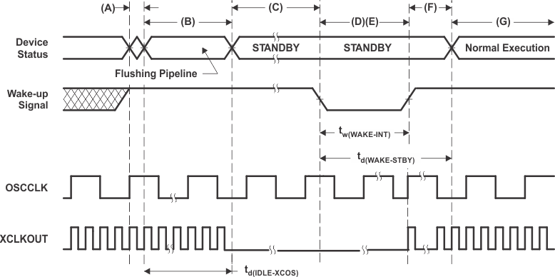
STANDBY Entry and Exit Timing Diagram
GUID-20210426-CA0I-CMVH-FZCM-6GL4CZMCCJKH-low.gif
IDLE instruction is executed to put the device into STANDBY mode.
The LPM block responds to the STANDBY signal, SYSCLK is held for a maximum 16 INTOSC1 clock cycles before being turned off. This delay enables the CPU pipeline and any other pending operations to flush properly.
Clock to the peripherals are turned off. However, the PLL and watchdog are not shut down. The device is now in STANDBY mode. After the IDLE instruction is executed, a delay of five OSCCLK cycles (minimum) is needed before the wake-up signal could be asserted.
The external wake-up signal is driven active.
The wake-up signal fed to a GPIO pin to wake up the device must meet the minimum pulse width requirement. Furthermore, this signal must be free of glitches. If a noisy signal is fed to a GPIO pin, the wake-up behavior of the device will not be deterministic and the device may not exit low-power mode for subsequent wake-up pulses.
After a latency period, the STANDBY mode is exited.
Normal execution resumes. The device will respond to the interrupt (if enabled).
Figure 6-39 STANDBY Entry and Exit Timing Diagram