JAJSH24D March 2019 – February 2024 TMUX1101 , TMUX1102
PRODUCTION DATA
- 1
- 1 特長
- 2 アプリケーション
- 3 概要
- 4 Device Comparison Table
- 5 Pin Configuration and Functions
-
6 Specifications
- 6.1 Absolute Maximum Ratings
- 6.2 ESD Ratings
- 6.3 Recommended Operating Conditions
- 6.4 Thermal Information
- 6.5 Electrical Characteristics (VDD = 5V ±10 %)
- 6.6 Electrical Characteristics (VDD = 3.3V ±10 %)
- 6.7 Electrical Characteristics (VDD = 1.8V ±10 %)
- 6.8 Electrical Characteristics (VDD = 1.2V ±10 %)
- 6.9 Typical Characteristics
- 7 Parameter Measurement Information
- 8 Detailed Description
- 9 Application and Implementation
- 10Device and Documentation Support
- 11Revision History
- 12Mechanical, Packaging, and Orderable Information
パッケージ・オプション
デバイスごとのパッケージ図は、PDF版データシートをご参照ください。
メカニカル・データ(パッケージ|ピン)
- DBV|5
- DCK|5
サーマルパッド・メカニカル・データ
発注情報
7.5 Charge Injection
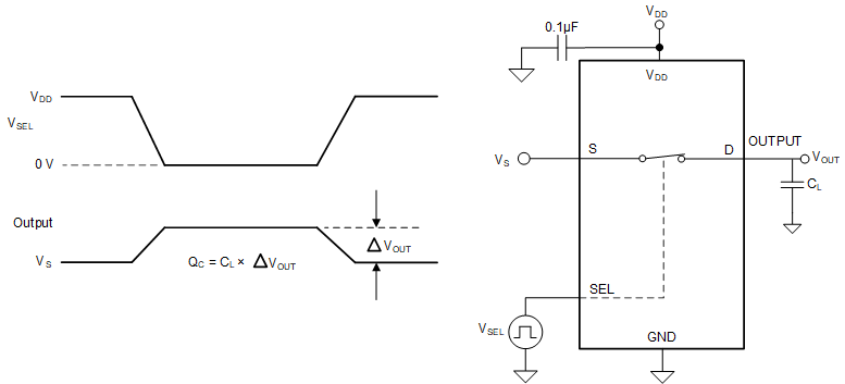
The TMUX110x devices have a transmission-gate topology. Any mismatch in capacitance between the NMOS and PMOS transistors results in a charge injected into the drain or source during the falling or rising edge of the gate signal. The amount of charge injected into the source or drain of the device is known as charge injection, and is denoted by the symbol QC. Figure 7-5 shows the setup used to measure charge injection from source (S) to drain (D).
 Figure 7-5 Charge-Injection
Measurement Setup