JAJSGN7A December 2018 – February 2024 TMUX1109
PRODUCTION DATA
- 1
- 1 特長
- 2 アプリケーション
- 3 概要
- 4 Pin Configuration and Functions
-
5 Specifications
- 5.1 Absolute Maximum Ratings
- 5.2 ESD Ratings
- 5.3 Recommended Operating Conditions
- 5.4 Thermal Information
- 5.5 Electrical Characteristics (VDD = 5V ±10 %)
- 5.6 Electrical Characteristics (VDD = 3.3V ±10 %)
- 5.7 Electrical Characteristics (VDD = 2.5V ±10 %), (VSS = –2.5V ±10 %)
- 5.8 Electrical Characteristics (VDD = 1.8V ±10 %)
- 5.9 Electrical Characteristics (VDD = 1.2V ±10 %)
- Typical Characteristics
- 6 Detailed Description
- 7 Application and Implementation
- 8 Device and Documentation Support
- 9 Revision History
- 10Mechanical, Packaging, and Orderable Information
パッケージ・オプション
デバイスごとのパッケージ図は、PDF版データシートをご参照ください。
メカニカル・データ(パッケージ|ピン)
- PW|16
- RSV|16
サーマルパッド・メカニカル・データ
発注情報
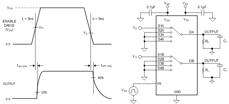
6.1.6 tON(EN) and tOFF(EN)
Turn-on time is defined as the time taken by the output of the device to rise to 10% after the enable has risen past the logic threshold. The 10% measurement is utilized to provide the timing of the device, system level timing can then account for the time constant added from the load resistance and load capacitance. Figure 6-6 shows the setup used to measure turn-on time, denoted by the symbol tON(EN).
Turn-off time is defined as the time taken by the output of the device to fall to 90% after the enable has fallen past the logic threshold. The 90% measurement is utilized to provide the timing of the device, system level timing can then account for the time constant added from the load resistance and load capacitance. Figure 6-6 shows the setup used to measure turn-off time, denoted by the symbol tOFF(EN).
 Figure 6-6 Turn-On and Turn-Off Time Measurement Setup