JAJSGY3C February 2019 – December 2023 TMUX1111 , TMUX1112 , TMUX1113
PRODUCTION DATA
- 1
- 1 特長
- 2 アプリケーション
- 3 概要
- 4 Device Comparison Table
- 5 Pin Configuration and Functions
-
6 Specifications
- 6.1 Absolute Maximum Ratings
- 6.2 ESD Ratings
- 6.3 Recommended Operating Conditions
- 6.4 Thermal Information
- 6.5 Electrical Characteristics (VDD = 5V ±10 %)
- 6.6 Electrical Characteristics (VDD = 3.3V ±10 %)
- 6.7 Electrical Characteristics (VDD = 1.8V ±10 %)
- 6.8 Electrical Characteristics (VDD = 1.2V ±10 %)
- 6.9 Typical Characteristics
- 7 Parameter Measurement Information
- 8 Detailed Description
- 9 Application and Implementation
- 10Device and Documentation Support
- 11Revision History
- 12Mechanical, Packaging, and Orderable Information
パッケージ・オプション
デバイスごとのパッケージ図は、PDF版データシートをご参照ください。
メカニカル・データ(パッケージ|ピン)
- PW|16
- RSV|16
サーマルパッド・メカニカル・データ
発注情報
7.2 Off-leakage current
There are two types of leakage currents associated with a switch during the off state:
- Source off-leakage current
- Drain off-leakage current
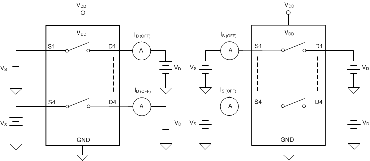
Source leakage current is defined as the leakage current flowing into or out of the source pin when the switch is off. This current is denoted by the symbol IS(OFF).
Drain leakage current is defined as the leakage current flowing into or out of the drain pin when the switch is off. This current is denoted by the symbol ID(OFF).
The setup used to measure both off-leakage currents is shown in Figure 7-2.
 Figure 7-2 Off-Leakage Measurement
Setup