JAJSGY3C February 2019 – December 2023 TMUX1111 , TMUX1112 , TMUX1113
PRODUCTION DATA
- 1
- 1 特長
- 2 アプリケーション
- 3 概要
- 4 Device Comparison Table
- 5 Pin Configuration and Functions
-
6 Specifications
- 6.1 Absolute Maximum Ratings
- 6.2 ESD Ratings
- 6.3 Recommended Operating Conditions
- 6.4 Thermal Information
- 6.5 Electrical Characteristics (VDD = 5V ±10 %)
- 6.6 Electrical Characteristics (VDD = 3.3V ±10 %)
- 6.7 Electrical Characteristics (VDD = 1.8V ±10 %)
- 6.8 Electrical Characteristics (VDD = 1.2V ±10 %)
- 6.9 Typical Characteristics
- 7 Parameter Measurement Information
- 8 Detailed Description
- 9 Application and Implementation
- 10Device and Documentation Support
- 11Revision History
- 12Mechanical, Packaging, and Orderable Information
パッケージ・オプション
デバイスごとのパッケージ図は、PDF版データシートをご参照ください。
メカニカル・データ(パッケージ|ピン)
- PW|16
- RSV|16
サーマルパッド・メカニカル・データ
発注情報
9.3 Typical Application - Switched Gain Amplifier
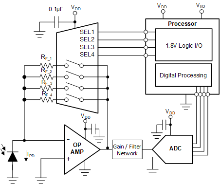
Switches and multiplexers are commonly used in the feedback path of amplifier circuits to provide configurable gain control. By using various resistor values on each switch path the TMUX111x allows the system to have multiple gain settings. An external resistor, or utilizing 1 channel always being closed, causes the amplifier to not operate in an open loop configuration. A transimpedance amplifier (TIA) for photodiode inputs is a common circuit that requires gain control using a multi-channel switch to convert the output current of the photodiode into a voltage for the MCU or processor. The leakage current, capacitance, and charge injection performance of the TMUX111x are key specifications to evaluate when selecting a device for gain control.
 Figure 9-5 Switching Gain Settings of a TIA circuit