JAJSUX4 June 2024 TMUX1308A , TMUX1309A
PRODUCTION DATA
- 1
- 1 特長
- 2 アプリケーション
- 3 概要
- 4 Device Comparison Table
- 5 Pin Configuration and Functions
-
6 Specifications
- 6.1 Absolute Maximum Ratings
- 6.2 ESD Ratings
- 6.3 Thermal Information: TMUX1308A
- 6.4 Thermal Information: TMUX1309A
- 6.5 Recommended Operating Conditions
- 6.6 Electrical Characteristics
- 6.7 Logic and Dynamic Characteristics
- 6.8 Timing Characteristics
- 6.9 Injection Current Coupling
- 6.10 Typical Characteristics
- 7 Parameter Measurement Information
-
8 Detailed Description
- 8.1 Overview
- 8.2 Functional Block Diagram
- 8.3
Feature Description
- 8.3.1 Bidirectional Operation
- 8.3.2 Rail-to-Rail Operation
- 8.3.3 1.8V Logic Compatible Inputs
- 8.3.4 Fail-Safe Logic
- 8.3.5 High-Impedance Optimization
- 8.3.6
Injection Current Control
- 8.3.6.1 TMUX13xxA is Powered, Channel is Unselected, and the Input Signal is Greater Than VDD (VDD = 5V, VINPUT = 5.5V)
- 8.3.6.2 TMUX13xxA is Powered, Channel is Selected, and the Input Signal is Greater Than VDD (VDD = 5V, VINPUT = 5.5V)
- 8.3.6.3 TMUX13xxA is Unpowered and the Input Signal has a Voltage Present (VDD = 0V, VINPUT = 3V)
- 8.4 Device Functional Modes
- 8.5 Truth Tables
- 9 Application and Implementation
- 10Device and Documentation Support
- 11Mechanical, Packaging, and Orderable Information
- 12Revision History
パッケージ・オプション
デバイスごとのパッケージ図は、PDF版データシートをご参照ください。
メカニカル・データ(パッケージ|ピン)
- PW|16
サーマルパッド・メカニカル・データ
発注情報
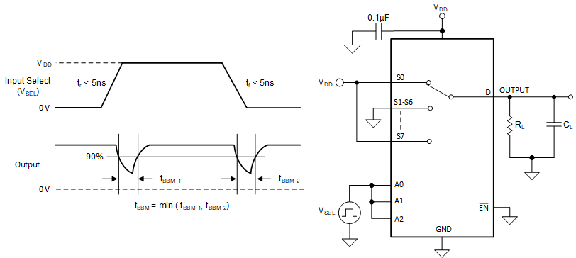
7.5 Break-Before-Make
Break-before-make delay is a safety feature that prevents two inputs from connecting when the device is switching. The output first breaks from the on-state switch before making the connection with the next on-state switch. The time delay between the break and the make is known as break-before-make delay. Figure 7-5 shows the setup used to measure break-before-make delay, denoted by the symbol tOPEN(BBM).
 Figure 7-5 Break-Before-Make Delay Measurement Setup