JAJSUX4 June 2024 TMUX1308A , TMUX1309A
PRODUCTION DATA
- 1
- 1 特長
- 2 アプリケーション
- 3 概要
- 4 Device Comparison Table
- 5 Pin Configuration and Functions
-
6 Specifications
- 6.1 Absolute Maximum Ratings
- 6.2 ESD Ratings
- 6.3 Thermal Information: TMUX1308A
- 6.4 Thermal Information: TMUX1309A
- 6.5 Recommended Operating Conditions
- 6.6 Electrical Characteristics
- 6.7 Logic and Dynamic Characteristics
- 6.8 Timing Characteristics
- 6.9 Injection Current Coupling
- 6.10 Typical Characteristics
- 7 Parameter Measurement Information
-
8 Detailed Description
- 8.1 Overview
- 8.2 Functional Block Diagram
- 8.3
Feature Description
- 8.3.1 Bidirectional Operation
- 8.3.2 Rail-to-Rail Operation
- 8.3.3 1.8V Logic Compatible Inputs
- 8.3.4 Fail-Safe Logic
- 8.3.5 High-Impedance Optimization
- 8.3.6
Injection Current Control
- 8.3.6.1 TMUX13xxA is Powered, Channel is Unselected, and the Input Signal is Greater Than VDD (VDD = 5V, VINPUT = 5.5V)
- 8.3.6.2 TMUX13xxA is Powered, Channel is Selected, and the Input Signal is Greater Than VDD (VDD = 5V, VINPUT = 5.5V)
- 8.3.6.3 TMUX13xxA is Unpowered and the Input Signal has a Voltage Present (VDD = 0V, VINPUT = 3V)
- 8.4 Device Functional Modes
- 8.5 Truth Tables
- 9 Application and Implementation
- 10Device and Documentation Support
- 11Mechanical, Packaging, and Orderable Information
- 12Revision History
パッケージ・オプション
デバイスごとのパッケージ図は、PDF版データシートをご参照ください。
メカニカル・データ(パッケージ|ピン)
- PW|16
サーマルパッド・メカニカル・データ
発注情報
9.2 Typical Application
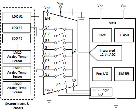
One useful application that takes advantage of the TMUX13xxA features is multiplexing various signals into an ADC that is integrated into an MCU. Utilizing an integrated ADC in an MCU allows a system to minimize cost with a potential tradeoff of system performance when compared to an external ADC. The multiplexer allows for multiple inputs or sensors to be monitored with a single ADC pin of the device, which is critical in systems with limited I/O. The TMUX1309A is an excellent choice for a similar design example using differential signals, or as two 4:1 multiplexers.
 Figure 9-1 Multiplexing Signals to Integrated ADC