JAJSK10B september 2021 – august 2023 TMUX8108 , TMUX8109
PRODUCTION DATA
- 1
- 1 特長
- 2 アプリケーション
- 3 概要
- 4 Revision History
- 5 Device Comparison Table
- 6 Pin Configuration and Functions
-
7 Specifications
- 7.1 Absolute Maximum Ratings: TMUX810x Devices
- 7.2 ESD Ratings
- 7.3 Recommended Operating Conditions: TMUX810x Devices
- 7.4 Thermal Information
- 7.5 Electrical Characteristics (Global): TMUX810x Devices
- 7.6 Electrical Characteristics (±15-V Dual Supply)
- 7.7 Electrical Characteristics (±36-V Dual Supply)
- 7.8 Electrical Characteristics (±50-V Dual Supply)
- 7.9 Electrical Characteristics (72-V Single Supply)
- 7.10 Electrical Characteristics (100-V Single Supply)
- 7.11 Switching Characteristics: TMUX810x Devices
- 7.12 Typical Characteristics
- 8 Parameter Measurement Information
- 9 Detailed Description
- 10Application and Implementation
- 11Device and Documentation Support
- 12Mechanical, Packaging, and Orderable Information
パッケージ・オプション
デバイスごとのパッケージ図は、PDF版データシートをご参照ください。
メカニカル・データ(パッケージ|ピン)
- PW|16
- RUM|16
サーマルパッド・メカニカル・データ
- RUM|16
発注情報
8.9 Crosstalk
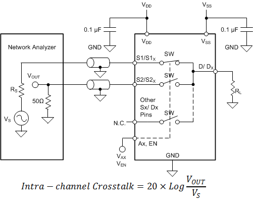
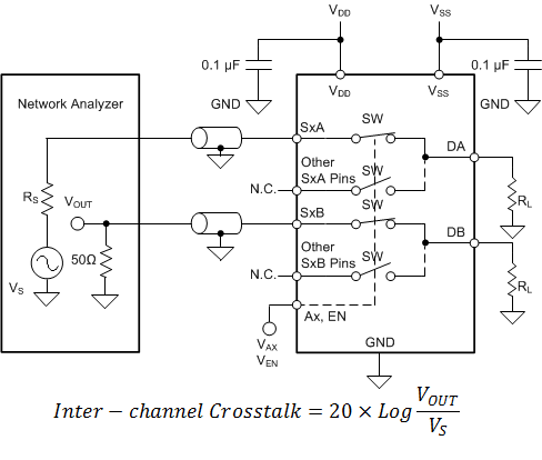
There are two types of crosstalk that can be defined for the devices:
- Intra-channel crosstalk (XTALK(INTRA)): the voltage at the source pin (Sx) of an off-switch input when a signal is applied at the source pin of an on-switch input in the same channel, as shown in Figure 8-9 .
- Inter-channel crosstalk (XTALK(INTER)): the voltage at the source pin (Sx) of an on-switch input when a signal is applied at the source pin of an on-switch input in a different channel, as shown in Figure 8-10. Inter-channel crosstalk applies only to the TMUX8109 device.
 Figure 8-9 Intra-channel Crosstalk Measurement Setup
 Figure 8-10 Inter-channel Crosstalk Measurement Setup