JAJSK10B september 2021 – august 2023 TMUX8108 , TMUX8109
PRODUCTION DATA
- 1
- 1 特長
- 2 アプリケーション
- 3 概要
- 4 Revision History
- 5 Device Comparison Table
- 6 Pin Configuration and Functions
-
7 Specifications
- 7.1 Absolute Maximum Ratings: TMUX810x Devices
- 7.2 ESD Ratings
- 7.3 Recommended Operating Conditions: TMUX810x Devices
- 7.4 Thermal Information
- 7.5 Electrical Characteristics (Global): TMUX810x Devices
- 7.6 Electrical Characteristics (±15-V Dual Supply)
- 7.7 Electrical Characteristics (±36-V Dual Supply)
- 7.8 Electrical Characteristics (±50-V Dual Supply)
- 7.9 Electrical Characteristics (72-V Single Supply)
- 7.10 Electrical Characteristics (100-V Single Supply)
- 7.11 Switching Characteristics: TMUX810x Devices
- 7.12 Typical Characteristics
- 8 Parameter Measurement Information
- 9 Detailed Description
- 10Application and Implementation
- 11Device and Documentation Support
- 12Mechanical, Packaging, and Orderable Information
パッケージ・オプション
デバイスごとのパッケージ図は、PDF版データシートをご参照ください。
メカニカル・データ(パッケージ|ピン)
- PW|16
- RUM|16
サーマルパッド・メカニカル・データ
- RUM|16
発注情報
10.2.3 Application Curves
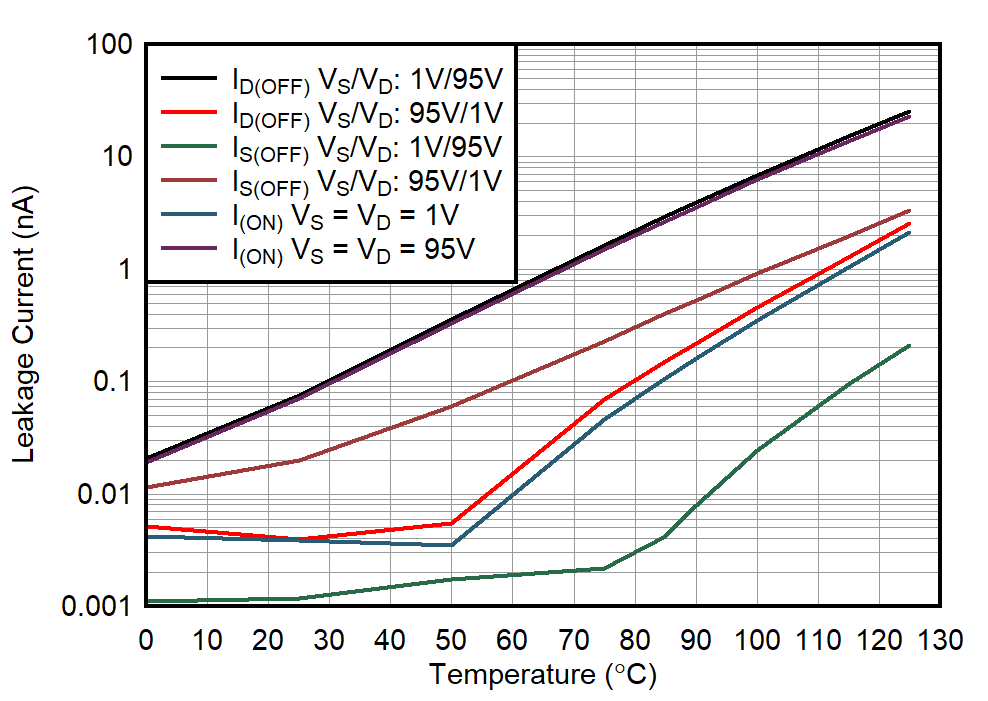
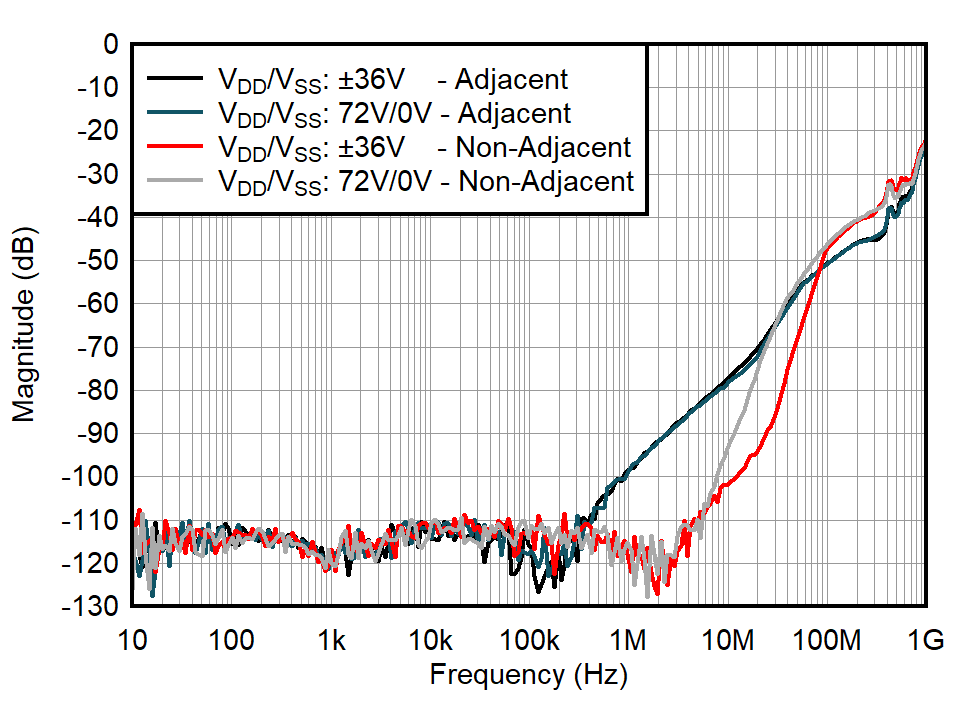
The example application utilizes the excellent leakage and crosstalk performance of the TMUX810x devices to reduce any impact introduced from a multiplexed system architecture. Figure 10-2 shows the leakage current for both ON and OFF cases with a varying temperature. Figure 10-3 shows the excellent crosstalk performance of the TMUX810x devices. These features make the TMUX8108 and TMUX8109 an excellent solution for multiplexed data acquisition applications that require excellent linearity and low distortion.

