JAJSQU4 july 2023 TMUXHS221LV
PRODUCTION DATA
- 1
- 1 特長
- 2 アプリケーション
- 3 概要
- 4 Revision History
- 5 Pin Configuration and Functions
-
6 Specifications
- 6.1 Absolute Maximum Ratings
- 6.2 ESD Ratings
- 6.3 Recommended Operating Conditions
- 6.4 Thermal Information
- 6.5 Electrical Characteristics
- 6.6 High-Speed Performance Parameters
- 6.7 Switching Characteristics
- 6.8 Typical Characteristics – S-Parameters
- 6.9 Typical Characteristics – RON
- 6.10 Typical Characteristics – Eye Diagrams
- 18
- 7 Detailed Description
- 8 Application and Implementation
- 9 Device and Documentation Support
- 10Mechanical, Packaging, and Orderable Information
8.2.1.3 Application Curves
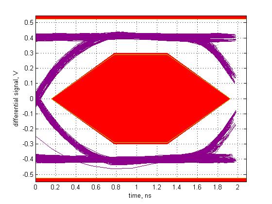
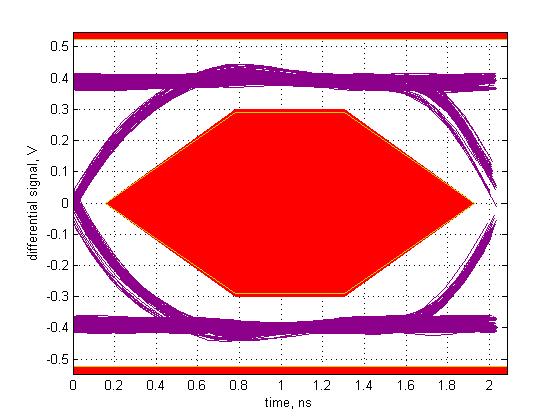
Figure 8-2 and Figure 8-3 show eye diagrams for USB 2.0 signals through calibration traces (without device) and TMUXHS221LV channel. A combination of very low channel ON resistance, high bandwidth, very low reflection (return loss), and low added jitter from the device allows 480Mbps USB 2.0 HS signals to remain unattenuated. Many system platforms struggle to pass USB 2.0 compliance due to high loss. TMUXHS221LV allows insertion of an analog mux device in the signal path without creating any additional signal integrity issues.
 Figure 8-2 USB 2.0 HS Compliance Eye in TI Evaluation Board – Through Calibration Traces
  Figure 8-3 USB 2.0 HS Compliance Eye in TI Evaluation Board – Through TMUXHS221LV Channel