SLOS275E January 2000 – November 2016 TPA0211
PRODUCTION DATA.
- 1 Features
- 2 Applications
- 3 Description
- 4 Revision History
- 5 Device Comparison Table
- 6 Pin Configuration and Functions
- 7 Specifications
- 8 Parameter Measurement Information
- 9 Detailed Description
- 10Application and Implementation
- 11Power Supply Recommendations
- 12Layout
- 13Device and Documentation Support
- 14Mechanical, Packaging, and Orderable Information
パッケージ・オプション
デバイスごとのパッケージ図は、PDF版データシートをご参照ください。
メカニカル・データ(パッケージ|ピン)
- DGN|8
サーマルパッド・メカニカル・データ
- DGN|8
発注情報
10 Application and Implementation
NOTE
Information in the following applications sections is not part of the TI component specification, and TI does not warrant its accuracy or completeness. TI’s customers are responsible for determining suitability of components for their purposes. Customers should validate and test their design implementation to confirm system functionality.
10.1 Application Information
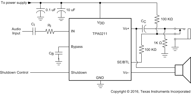
These typical connection diagrams highlight the required external components and system level connections for proper operation of the device. Each of these configurations can be realized using the Evaluation Modules (EVMs) for the device. These flexible modules allow full evaluation of the device in the most common modes of operation. Any design variation can be supported by TI through schematic and layout reviews. Visit e2e.ti.com for design assistance and join the audio amplifier discussion forum for additional information.
10.2 Typical Application
 Figure 27. TPA0211 With SE/BTL Operation
10.2.1 Design Requirements
For this example, Table 4 lists the design parameters.
Table 4. Design Parameters
| PARAMETER | VALUE |
|---|---|
| Power supply | 5 V |
| Enable inputs | High > 2 V |
| Low < 0.8 V | |
| Speaker | 8 Ω |
10.2.2 Detailed Design Procedure
10.2.2.1 Surface Mount Capacitor
Low-ESR capacitors are recommended throughout this applications section. A real (as opposed to ideal) capacitor can be modeled simply as a resistor in series with an ideal capacitor. The voltage drop across this resistor minimizes the beneficial effects of the capacitor in the circuit. The lower the equivalent value of this resistance the more the real capacitor behaves like an ideal capacitor.
Temperature and applied DC voltage influence the actual capacitance of high-K materials. Table 5 shows the relationship between the different types of high-K materials and their associated tolerances, temperature coefficients, and temperature ranges. Notice that a capacitor made with X5R material can lose up to 15% of its capacitance within its working temperature range.
In an application, the working capacitance of components made with high-K materials is generally much lower than nominal capacitance. A worst case result with a typical X5R material might be –10% tolerance, –15% temperature effect, and –45% DC voltage effect at 50% of the rated voltage. This particular case would result in a working capacitance of 42% (0.9 × 0.85 × 0.55) of the nominal value.
Select high-K ceramic capacitors according to the following rules:
- Use capacitors made of materials with temperature coefficients of X5R, X7R, or better.
- Use capacitors with DC voltage ratings of at least twice the application voltage. Use minimum 10-V capacitors for this device.
- Choose a capacitance value at least twice the nominal value calculated for the application. Multiply the nominal value by a factor of 2 for safety. If a 10-µF capacitor is required, use 20 µF.
The preceding rules and recommendations apply to capacitors used in connection with the device. This device cannot meet its performance specifications if the rules and recommendations are not followed.
Table 5. Typical Tolerance and Temperature Coefficient of Capacitance by Material
| MATERIAL | TYPICAL TOLERANCE | TEMPERATURE | TEMPERATURE RANGE (°C) |
|---|---|---|---|
| COG/NOP | ±5% | ±30 ppm | –55 to 125 |
| X7R | ±10% | ±15% | –55 to 125 |
| X5R | 80% to –20% | 22% to –82% | –30 to 85 |
10.2.2.2 Input Capacitor, Ci
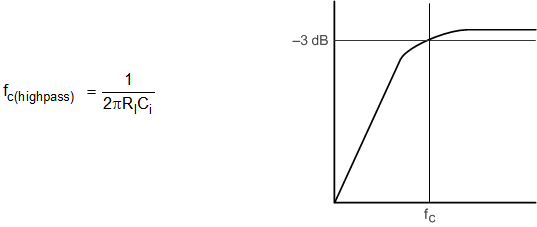
In the typical application an input capacitor, Ci, is required to allow the amplifier to bias the input signal to the proper dc level for optimum operation. In this case, Ci and the input resistance of the amplifier, RI, form a high-pass filter with the corner frequency determined in Equation 11.

The value of Ci is important to consider as it directly affects the bass (low frequency) performance of the circuit. Consider the example where RI is 10 kΩ and the specification calls for a flat bass response down to 40 Hz. Equation 6 is reconfigured as Equation 12.

In this example, CI is 0.4 µF so one would likely choose a value in the range of 0.47 µF to 1 µF. A further consideration for this capacitor is the leakage path from the input source through the input network (Ci) and the feedback network to the load. This leakage current creates a dc offset voltage at the input to the amplifier that reduces useful headroom, especially in high gain applications. For this reason a low-leakage tantalum or ceramic capacitor is the best choice. When polarized capacitors are used, the positive side of the capacitor should face the amplifier input in most applications as the dc level there is held at VDD/2, which is likely higher than the source dc level. Note that it is important to confirm the capacitor polarity in the application.
10.2.2.3 Power Supply Decoupling, C(S)
The TPA0211 is a high-performance CMOS audio amplifier that requires adequate power supply decoupling to ensure the output total harmonic distortion (THD) is as low as possible. Power supply decoupling also prevents oscillations for long lead lengths between the amplifier and the speaker. The optimum decoupling is achieved by using two capacitors of different types that target different types of noise on the power supply leads. For higher frequency transients, spikes, or digital hash on the line, a good low equivalent-series-resistance (ESR) ceramic capacitor, typically 0.1 µF placed as close as possible to the device VDD lead, works best. For filtering lower-frequency noise signals, TI recommends a larger aluminum electrolytic capacitor of 10 µF or greater placed near the audio power amplifier.
10.2.2.4 Midrail Bypass Capacitor, C(BYP)
The midrail bypass capacitor, C(BYP), is the most critical capacitor and serves several important functions. During start-up or recovery from shutdown mode, C(BYP) determines the rate at which the amplifier starts up. The second function is to reduce noise produced by the power supply caused by coupling into the output drive signal. This noise is from the midrail generation circuit internal to the amplifier, which appears as degraded PSRR and THD+N.
Bypass capacitor, C(BYP), values of 0.47 µF to 1 µF ceramic or tantalum low-ESR capacitors are recommended for the best THD and noise performance.
10.2.2.5 Output Coupling Capacitor, C(C)
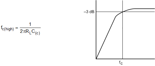
In the typical single-supply SE configuration, an output coupling capacitor (C(C)) is required to block the dc bias at the output of the amplifier thus preventing dc currents in the load. As with the input coupling capacitor, the output coupling capacitor and impedance of the load form a high-pass filter governed by Equation 13.

The main disadvantage, from a performance standpoint, is that the load impedances are typically small, which drives the low-frequency corner higher, degrading the bass response. Large values of C(C) are required to pass low frequencies into the load. Consider the example where a C(C) of 330 µF is chosen and loads vary from 3 Ω, 4 Ω, 8 Ω, 32 Ω, 10 kΩ, to 47 kΩ. Table 6 summarizes the frequency response characteristics of each configuration.
Table 6. Common Load Impedances vs Low Frequency Output Characteristics in SE Mode
| RL | C(C) | LOWEST FREQUENCY |
|---|---|---|
| 3 Ω | 330 µF | 161 Hz |
| 4 Ω | 330 µF | 120 Hz |
| 8 Ω | 330 µF | 60 Hz |
| 32 Ω | 330 µF | 15 Hz |
| 10,000 Ω | 330 µF | 0.05 Hz |
| 47,000 Ω | 330 µF | 0.01 Hz |
As Table 6 indicates, most of the bass response is attenuated into a 4-Ω load, an 8-Ω load is adequate, headphone response is good, and drive into line level inputs (a home stereo for example) is exceptional.
Furthermore, the total amount of ripple current that must flow through the capacitor must be considered when choosing the component. As shown in the application circuit, one coupling capacitor must be in series with the mono loudspeaker for proper operation of the stereo-mono switching circuit. For a 4-Ω load, this capacitor must be able to handle about 700 mA of ripple current for a continuous output power of 2 W.
10.2.3 Application Curves
Table 7 lists the figures for the application curves.