SLOS474E August 2005 – March 2016 TPA2005D1-Q1
PRODUCTION DATA.
- 1 Features
- 2 Applications
- 3 Description
- 4 Revision History
- 5 Device Comparison Table
- 6 Pin Configuration and Functions
- 7 Specifications
- 8 Parameter Measurement Information
- 9 Detailed Description
- 10Application and Implementation
- 11Power Supply Recommendations
- 12Layout
- 13Device and Documentation Support
- 14Mechanical, Packaging, and Orderable Information
パッケージ・オプション
メカニカル・データ(パッケージ|ピン)
サーマルパッド・メカニカル・データ
発注情報
7 Specifications
7.1 Absolute Maximum Ratings
over operating free-air temperature range (unless otherwise noted)(1)| MIN | MAX | UNIT | |||
|---|---|---|---|---|---|
| VDD | Supply voltage(2) | In active mode | –0.3 | 6 | V |
| In SHUTDOWN mode | –0.3 | 7 | V | ||
| VI | Input voltage | –0.3 | VDD + 0.3 V | V | |
| RL | Load resistance | 2.5 ≤ VDD ≤ 4.2 V | 3.2 | Ω | |
| 4.2 < VDD ≤ 6 V | 6.4 | Ω | |||
| TA | Operating free-air temperature | Non T-suffix | –40 | 85 | °C |
| T-suffix | –40 | 105 | |||
| TJ | Operating junction temperature | –40 | 150 | °C | |
| Tstg | Storage temperature | –65 | 150 | °C | |
(1) Stresses beyond those listed under Absolute Maximum Ratings may cause permanent damage to the device. These are stress ratings only, which do not imply functional operation of the device at these or any other conditions beyond those indicated under Recommended Operating Conditions. Exposure to absolute-maximum-rated conditions for extended periods may affect device reliability.
(2) For the MSOP (DGN) package option, the maximum VDD should be limited to 5 V if short-circuit protection is desired.
7.2 ESD Ratings
| VALUE | UNIT | |||
|---|---|---|---|---|
| V(ESD) | Electrostatic discharge | Human-body model (HBM), per AEC Q100-002(1) | ±2000 | V |
| Charged-device model (CDM), per AEC Q100-011 | ±1000 | |||
(1) AEC Q100-002 indicates that HBM stressing shall be in accordance with the ANSI/ESDA/JEDEC JS-001 specification.
7.3 Recommended Operating Conditions
| MIN | MAX | UNIT | |||
|---|---|---|---|---|---|
| VDD | Supply voltage | 2.5 | 5.5 | V | |
| VIH | High-level input voltage | SHUTDOWN | 2 | VDD | V |
| VIL | Low-level input voltage | SHUTDOWN | 0 | 0.7 | V |
| RI | Input resistor | Gain ≤ 20 V/V (26 dB) | 15 | kΩ | |
| VIC | Common-mode input voltage | VDD = 2.5 V, 5.5 V, CMRR ≤ –49 dB | 0.5 | VDD – 0.8 | V |
| TA | Operating free-air temperature | Non T-suffix | –40 | 85 | °C |
| T-suffix | –40 | 105 | |||
7.4 Thermal Information
| THERMAL METRIC(1) | TPA2005D1-Q1 | UNIT | ||
|---|---|---|---|---|
| DRB (SON) | DGN (MSOP PowerPAD) |
|||
| 8 PINS | 8 PINS | |||
| RθJA | Junction-to-ambient thermal resistance | 49.5 | 57 | °C/W |
| RθJC(top) | Junction-to-case (top) thermal resistance | 62.1 | 53.8 | °C/W |
| RθJB | Junction-to-board thermal resistance | 24.8 | 33.7 | °C/W |
| ψJT | Junction-to-top characterization parameter | 1.3 | 1.9 | °C/W |
| ψJB | Junction-to-board characterization parameter | 24.9 | 33.4 | °C/W |
| RθJC(bot) | Junction-to-case (bottom) thermal resistance | 6.9 | 6.4 | °C/W |
(1) For more information about traditional and new thermal metrics, see the Semiconductor and IC Package Thermal Metrics application report, SPRA953.
7.5 Electrical Characteristics
TA = –40°C to 85°C (unless otherwise noted)| PARAMETER | TEST CONDITIONS | MIN | TYP | MAX | UNIT | ||
|---|---|---|---|---|---|---|---|
| |VOS| | Output offset voltage (measured differentially) | VI = 0 V, AV = 2 V/V, VDD = 2.5 V to 5.5 V | 25 | mV | |||
| PSRR | Power-supply rejection ratio | VDD = 2.5 V to 5.5 V | –75 | –55 | dB | ||
| CMRR | Common-mode rejection ratio | VDD = 2.5 V to 5.5 V, VIC = VDD / 2 to 0.5 V, VIC = VDD / 2 to VDD – 0.8 V |
TA = 25°C | –68 | –49 | dB | |
| TA = –40°C to 85°C | –35 | ||||||
| |IIH| | High-level input current | VDD = 5.5 V, VI = 5.8 V | 50 | μA | |||
| |IIL| | Low-level input current | VDD = 5.5 V, VI = 0.3 V | TA = –40°C to 85°C | 4 | μA | ||
| TA = –40°C to 105°C | 12 | ||||||
| I(Q) | Quiescent current | VDD = 5.5 V, no load | 3.4 | 4.5 | mA | ||
| VDD = 3.6 V, no load | 2.8 | ||||||
| VDD = 2.5 V, no load | 2.2 | 3.2 | |||||
| I(SD) | Shutdown current | V (SHUTDOWN) = 0.8 V, VDD = 2.5 V to 5.5 V |
TA = –40°C to 85°C | 0.5 | 2 | μA | |
| TA = –40°C to 105°C | 2.5 | ||||||
| rDS(on) | Static drain-source on-state resistance | VDD = 2.5 V | 770 | mΩ | |||
| VDD = 3.6 V | 590 | ||||||
| VDD = 5.5 V | 500 | ||||||
| Output impedance in SHUTDOWN | V (SHUTDOWN) = 0.8 V | >1 | kΩ | ||||
| f(sw) | Switching frequency | VDD = 2.5 V to 5.5 V | 200 | 250 | 300 | kHz | |
| Gain |
 |
 |
 |
 |
|||
7.6 Operating Characteristics
TA = 25°C, Gain = 2 V/V, RL = 8 Ω (unless otherwise noted)| PARAMETER | TEST CONDITIONS | MIN | TYP | MAX | UNIT | ||
|---|---|---|---|---|---|---|---|
| PO | Output power | THD + N= 1%, f = 1 kHz, RL = 8 Ω |
VDD = 5 V | 1.18 | W | ||
| VDD = 3.6 V | 0.58 | ||||||
| VDD = 2.5 V | 0.26 | ||||||
| THD + N= 10%, f = 1 kHz, RL = 8 Ω |
VDD = 5 V | 1.45 | |||||
| VDD = 3.6 V | 0.75 | ||||||
| VDD = 2.5 V | 0.35 | ||||||
| THD+N | Total harmonic distortion plus noise | PO = 1 W, f = 1 kHz, RL = 8 Ω | VDD = 5 V | 0.18% | |||
| PO = 0.5 W, f = 1 kHz, RL = 8 Ω | VDD = 3.6 V | 0.19% | |||||
| PO = 200 mW, f = 1 kHz, RL = 8 Ω | VDD = 2.5 V | 0.20% | |||||
| kSVR | Supply ripple rejection ratio | f = 217 Hz, V(RIPPLE) = 200 mVpp, Inputs ac-grounded with Ci = 2 μF |
VDD = 3.6 V | –71 | dB | ||
| SNR | Signal-to-noise ratio | PO= 1 W, RL = 8 Ω | VDD = 5 V | 97 | dB | ||
| Vn | Output voltage noise | VDD = 3.6 V, f = 20 Hz to 20 kHz, Inputs ac-grounded with Ci = 2 μF |
No weighting | 48 | μVRMS | ||
| A weighting | 36 | ||||||
| CMRR | Common-mode rejection ratio | VIC = 1 Vpp , f = 217 Hz | VDD = 3.6 V | –63 | dB | ||
| ZI | Input impedance | 142 | 150 | 158 | kΩ | ||
| Start-up time from shutdown | VDD = 3.6 V | 9 | ms | ||||
7.7 Typical Characteristics
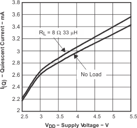
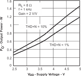
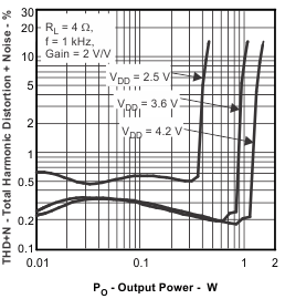
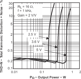 Figure 15. Total Harmonic Distortion + Noise vs Output Power
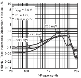
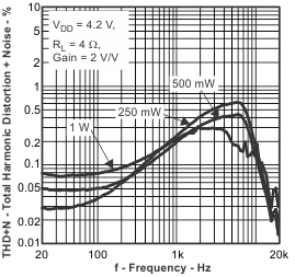
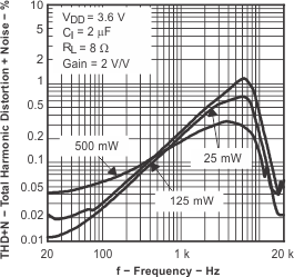 Figure 17. Total Harmonic Distortion + Noise vs Frequency
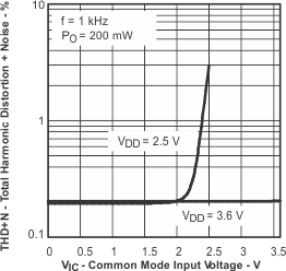
Common Mode Input Voltage
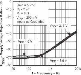
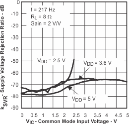
Common-Mode Input Voltage
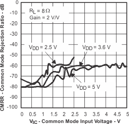 Figure 29. Common-Mode Rejection Ratio vs
 Common-Mode Input Voltage
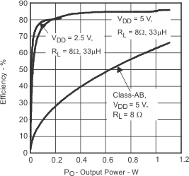
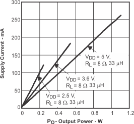
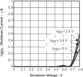
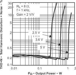 Figure 14. Total Harmonic Distortion + Noise vs Output Power
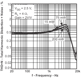
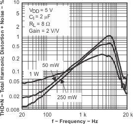 Figure 16. Total Harmonic Distortion + Noise vs Frequency
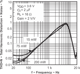
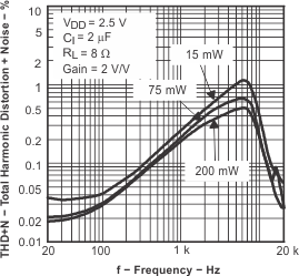 Figure 18. Total Harmonic Distortion + Noise vs Frequency
