SLOS650F August 2009 – June 2016 TPA3113D2
PRODUCTION DATA.
- 1 Features
- 2 Applications
- 3 Description
- 4 Revision History
- 5 Pin Configuration and Functions
-
6 Specifications
- 6.1 Absolute Maximum Ratings
- 6.2 ESD Ratings
- 6.3 Recommended Operating Conditions
- 6.4 Thermal Information
- 6.5 DC Electrical Characteristics, VCC = 24 V
- 6.6 DC Electrical Characteristics, VCC = 12 V
- 6.7 AC Electrical Characteristics, VCC = 24 V
- 6.8 AC Electrical Characteristics, VCC = 12 V
- 6.9 Typical Characteristics
- 7 Detailed Description
-
8 Application and Implementation
- 8.1 Application Information
- 8.2
Typical Applications
- 8.2.1
Stereo Class-D Amplifier With BTL Output
- 8.2.1.1 Design Requirements
- 8.2.1.2
Detailed Design Procedure
- 8.2.1.2.1 Ferrite Bead Filter Considerations
- 8.2.1.2.2 Efficiency: LC Filter Required With the Traditional Class-D Modulation Scheme
- 8.2.1.2.3 When to Use an Output Filter for EMI Suppression
- 8.2.1.2.4 Input Resistance
- 8.2.1.2.5 Input Capacitor, CI
- 8.2.1.2.6 BSN and BSP Capacitors
- 8.2.1.2.7 Differential Inputs
- 8.2.1.2.8 Using LOW-ESR Capacitors
- 8.2.1.3 Application Curves
- 8.2.2 Stereo Class-D Amplifier With BTL Output
- 8.2.3 Stereo Class-D Amplifier With PBTL Output
- 8.2.1
Stereo Class-D Amplifier With BTL Output
- 9 Power Supply Recommendations
- 10Layout
- 11Device and Documentation Support
- 12Mechanical, Packaging, and Orderable Information
パッケージ・オプション
メカニカル・データ(パッケージ|ピン)
- PWP|28
サーマルパッド・メカニカル・データ
- PWP|28
発注情報
1 Features
- 6-W/ch into an 8-Ω Loads at 10% THD+N From a 10-V Supply
- 12-W into a 4-Ω Mono Load at 10% THD+N From a 10-V Supply
- 87% Efficient Class-D Operation Eliminates Need for Heat Sinks
- Wide Supply Voltage Range Allows Operation from 8 V to 26 V
- Filter-Free Operation
- SpeakerGuard™ Speaker Protection Includes Adjustable Power Limiter Plus DC Protection
- Flow-Through Pinout Facilitates Easy Board Layout
- Robust Pin-to-Pin Short-Circuit Protection and Thermal Protection With Auto Recovery Option
- Excellent THD+N and Pop-Free Performance
- Four Selectable, Fixed Gain Settings
- Differential Inputs
2 Applications
- Televisions
- Consumer Audio Equipment
- Monitors
3 Description
The TPA3113D2 is a 6-W (per channel) efficient, Class-D audio power amplifier for driving bridged-tied stereo speakers. Advanced EMI Suppression Technology enables the use of inexpensive ferrite bead filters at the outputs while meeting EMC requirements. SpeakerGuard™ speaker protection circuitry includes an adjustable power limiter and a DC detection circuit. The adjustable power limiter allows the user to set a virtual voltage rail lower than the chip supply to limit the amount of current through the speaker. The DC detect circuit measures the frequency and amplitude of the PWM signal and shuts off the output stage if the input capacitors are damaged or shorts exist on the inputs.
The TPA3113D2 can drive stereo speakers as low as 4 Ω. The high efficiency of the TPA3113D2, 87%, eliminates the need for an external heat sink when playing music.
The outputs are also fully protected against shorts to GND, VCC, and output-to-output. The short-circuit protection and thermal protection includes an auto-recovery feature.
Device Information(1)
| PART NUMBER | PACKAGE | BODY SIZE (NOM) |
|---|---|---|
| TPA3113D2 | TSSOP (28) | 9.70 mm × 4.40 mm |
- For all available packages, see the orderable addendum at the end of the data sheet.
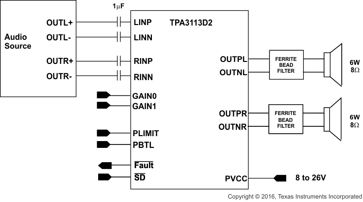
TPA3113D2 Simplified Application Schematic
